

Thanks! That's 3x confirmed. Couple more of confirms and we'll make it to the OP!Originally Posted by playground


Thanks! That's 3x confirmed. Couple more of confirms and we'll make it to the OP!
Maximus 5 Gene | i7-3770K @ 5GHz | ADATA 2x2GB @ 2.6GHz 9-12-10-28-1T | HD7970 @ 1200/6400
Rampage 4 Extreme | i7-3930K @ 5GHz ||| X58-A OC Orange | i7-980X @ 4.6GHz
it's my memory, it's just not liking the speeds.
i did prime95 for 17 hours straight @ 4.1ghz / 1800 memory and it was rock solid... then i restart, come back and i start playing World of Warcraft... 15 minutes into it windows crashes...
lowered memory back down to 1600 stock and no issues. haven't tested cpu stability any higher yet though. as it is, with RealTEMP, the cores are only seeing a max of 60-61*c on 4.1 so i'll see if it'll push higher.
Try bumping up VTT (QPI/DRAM) a little bit. I had in-game instabilities when first started playing with X58. Everything seemed fine, but when I start playing Crysis - BSOD.Raised VTT and everything was fine!
Raising IOH a bit might help also.
Maximus 5 Gene | i7-3770K @ 5GHz | ADATA 2x2GB @ 2.6GHz 9-12-10-28-1T | HD7970 @ 1200/6400
Rampage 4 Extreme | i7-3930K @ 5GHz ||| X58-A OC Orange | i7-980X @ 4.6GHz

what does that tell you about prime95
it's not my VTT, regardless if i raise it up to 1.55v even, it still will not stabilize and it's because of the memory
G.Skill F3-12800CL7D-4GBECO sticks are designed to run in pairs, not in groups of 6. i'm already pushing the voltage on them when they're stock voltage is 1.35v and i'm setting it to 1.61v for my current stable clocks.
so what i'm going to do is wait for GEIL to source out their GET312GB2000C8HC and GET312GB2000C9HC 6 stick kits that are designed to be stable at 2000mhz @ 1.65v at CL8 and CL9 stock settings using all 6 sticks for a 12gb setup and i've already confirmed with them that this kit is 100% stable on the RE3 + 980x build.
until then...
my stable clocking is:
4.54ghz @ 1.48v 34x133 ratio
1600mhz @ 7-8-7-24-72 (stock rated speed and timings on memory)
vTT - 1.5v, vDIM - 1.61v
what would be the best OCing BIOS?
just got the board yesterday and have BIOS 0402 which I see is the first bios...
Also, what is about the max BCLK everyone seems to be getting? I didnt look at all 67 pages ... but from what i got with my board seems to lock up at 221?
Last edited by The Duke; 07-16-2010 at 09:26 AM.
Intel I7 920 @ 4.3 // ASUS Rampage III Extreme// 3x2GB Mushkin// Antec TPQ 1200w // Water Cooled
if you're lucky that is with a good cpu and data link set to slow mode i think is how they're doing it.
but it depends on the cpu you're using.
as for bios i'd put 0704 on BIOS1 and put 0860 on BIOS2 and see what differences you can come up with. in a general look, the 4-4.5ghz range is pretty normal if you look at everything in an average, excluding LN2 clockers...
Seriously just get yourself some Corsair Ram. Ive got a kit of Dominator 2000Mhz C8 and I run it at 2000Mhz 8,8,8,24 CR2 1.65v 24/7 with RIII Extreme and 980X at 4.3Ghz 143x30 Vcore: 1.3750v, QPI: 1.23750. Ive pushed the memory further to around 2100mhz with a few more increments voltage without any trouble. Not sure how 12GB would go but it should be fine with a bit more voltage.
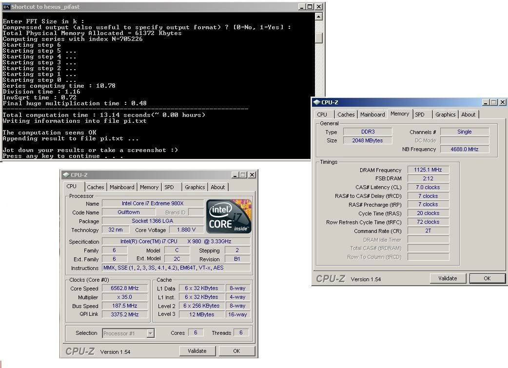
I did this one tonight with the mem at only 1.76v on LN2.. It was actually an accident..
RAM on Air?
What RAM did you use?
i7 920/950/w3565 @ ek hf
R3E @ bios 0602/0704
bbse gs 2133ps/hyper pdp2kc8 stt2kc8 stt2kc7 stt2.2kc8
zotec gtx480 @ stock @ pcie x8
x-fi elite pro @ pci
areca arc-1300-4e eSATAx4 controller @ pcie x1(x8)
hd*N @ ahci
corsair hx850w
cosmos rc-1000 case
windows xp pro 32-bit sp3/windows 7 ult 64-bit
Best settings to get an i7 920 D0 to 4.5GHz stable for 24/7 use?
\Project\ Triple Surround Fury
Case: Mountain Mods Ascension (modded)
CPU: i7 920 @ 4GHz + EK Supreme HF (plate #1)
GPU: GTX 670 3-Way SLI + XSPC Razor GTX670 water blocks
Mobo: ASUS Rampage III Extreme + EK FB R3E water block
RAM: 3x 2GB Mushkin Enhanced Ridgeback DDR3 @ 6-8-6-24 1T
SSD: Crucial M4 256GB, 0309 firmware
PSU: 2x Corsair HX1000s on separate circuits
LCD: 3x ASUS VW266H 26" Nvidia Surround @ 6030 x 1200
OS: Windows 7 64-bit Home Premium
Games: AoE II: HD, BF4, MKKE, MW2 via FourDeltaOne (Domination all day!)
he said nitro "I did this one tonight with the mem at only 1.76v on LN2"
or i can simply just wait a few weeks and get a full 6 stick kit for 12gb and have it fully stable at CL8, 2000mhz, 1.65v and around 1.25-1.3v qpi and not have to fine tune as much... the kit has already been tested according to the email i got from GEIL on the RE3. so it's not a big deal to just wait a bit... 1600 @ CL7 isn't bad in the mean time.
Last edited by skuldarin; 07-15-2010 at 11:28 PM.
But I don't think 1.76v 2250 777 is very impressive for RAM on LN2.
i7 920/950/w3565 @ ek hf
R3E @ bios 0602/0704
bbse gs 2133ps/hyper pdp2kc8 stt2kc8 stt2kc7 stt2.2kc8
zotec gtx480 @ stock @ pcie x8
x-fi elite pro @ pci
areca arc-1300-4e eSATAx4 controller @ pcie x1(x8)
hd*N @ ahci
corsair hx850w
cosmos rc-1000 case
windows xp pro 32-bit sp3/windows 7 ult 64-bit
his ram is on air (cmgtx2), cpu on ln2
bo do you see any real hit using single channel? Probably not at that speed
This is most auto overclockable board I've seen. I try everything on auto except multiplier 21 and bclk 207 and it pass 5 loops LinX (in very hot room)


Last edited by nickless; 07-16-2010 at 05:57 AM.
|RIIIE||Xeon W3520#3845A935|EVGA GTX480||PC3 16000 Kingston HyperX 6GB||2x150GB WD VRaptor||WD6401AALS||HAF 932//CM 1250W||LenovoL220x||X-Fi Xtreme Music||Lycosa+Lachesis+Destructor+G27+P880|
WC-Loop1: CPU |EK-Supreme HF|Magicool Xtreme III||MCP355||MCRES| Loop2: VGA/NB| EK-FC480 GTX-Acetal / MCW30|MCP655|MCR220QP|MCRES|
I received my RIIIE today - doing the build now.
Just a quick question regarding the 2 8pin 12v plugs ... I'm using a Corsair HW1000 .... should I plug in one of the 8 pin PCI-E 12v plugs also? Or can I just run with one 12v?
NZXT H440 & custom H2o | Asus Rampage III Extreme x58 | i7 980x @ 4.5GHz 1.3v 24/7 | SLI GTX780Ti | 12GB Corsair Dominator GT @2000MHz | 3 x Samsung s27a950's in 120hz Nvidia Surround 5760 x 1080 |
I dont think the 8pin pcie-e would fit, you shouldnt do that anyways. Single 8pin cpu is fine
they are there for when you run like tri/quad SLI/xfire to help with power issues ... normal use you only need to plug in 1
Intel I7 920 @ 4.3 // ASUS Rampage III Extreme// 3x2GB Mushkin// Antec TPQ 1200w // Water Cooled
I confirm that, 8 pin PCIE wont work, they dont have the same connectors as the CPu 8 Pin connector, I tried it once and had to return the extension cables, but I think if you change the connector only it will work. Just be sure to put the yellow and black wires at their proper position . Both of my CPU 8 Pins plugs are used and dont notice any difference from a single one. I guess its for heavy overclocking. Is it bad if I have both plugged..
@Toritechie ,
here is my template for 4.3 Ghz, its from BIOS 704...dont have much time to do more overclocking but I plan to try the newest BIOS on my second BIOS Chip..Its summer and I dont spend much time on my PC..
Good Luck with your new board
Code:Target CPU Frequency 4294MHz Target DRAM Frequency 1636MHz LN2 Mode [No]*** QPI Loadline Calibration [Yes]*** Sync Mode [Enabled] AI Overclock Tuner [Manual] OC From CPU level Up [Auto] CPU Ratio Setting [21] CPU Turbo Power Limit [Disabled] >CPU Configuration---------------------------- CPU Ratio Setting [21] C1E Support [Disabled] Hardware Prefetcher [Enabled] Adjacent Cache Line Prefetcher [Enabled] Intel(R) Virtualiyation Tech [Enabled] CPU TM Function [Disabled] Execute Disable Bit [Disabled] Intel(R) HT Technology [Enabled] Active Processor Cores [*ALL] A20M [Disabled] Intel(R) SpeedStep(TM) Tech [Disabled] Intel(R) C-STATE Tech [Disabled] C State package limit setting [Auto] ---------------------------------------------- BCLK Frequency [204] PCIE Frequency [102] DRAM Frequency [1636] UCLK Frequency [3672] QPI Link Data Rate [Auto] Memory Configuration Protect [Disabled] >DRAM Timing Control-------------------------- CAS# Latency [7] RAS# to CAS# Delay [8] RAS# PRE Time [7] RAS# ACT Time [18] RAS# to RAS# Delay [Auto] REF Cycle Time [72] WRITE Recovery Time [Auto] READ to PRE Time [Auto] FOUR ACT WIN Time [Auto] Back-To-BackCAS# Delay [Auto] Timing Mode [1N] Round Trip Latency on CHA [Auto] Round Trip Latency on CHB [Auto] Round Trip Latency on CHC [Auto] WRITE To READ Delay(DD) [Auto] WRITE To READ Delay(DR) [Auto] WRITE To READ Delay(SR) [Auto] READ To WRITE Delay(DD) [Auto] READ To WRITE Delay(DR) [Auto] READ To WRITE Delay(SR) [Auto] READ To READ Delay(DD) [Auto] READ To READ Delay(DR) [Auto] READ To READ Delay(SR) [Auto] WRITE To WRITE Delay(DD) [Auto] WRITE To WRITE Delay(DR) [Auto] WRITE To WRITE Delay(SR) [Auto] ---------------------------------------------- CPU Differential Amplitude [Auto] CPU Clock Skew [Auto] IOH Clock Skew [Auto] ------------ Extreme Engine Digi+ ------------ Digi+ PWR Mode [T-Balanced] PWR Volt. Control [Auto] Load-Line Calibration [Auto] CPU Voltege OCP [Enabled] CPU PWM Frequency [Auto] Extreme OV [Disabled] Extreme OC [Disabled] CPU Voltage [1.35v] CPU PLL Voltage [1.55025v] QPI/DRAM Core Voltage [1.30625v] DRAM Bus Voltage [1.65625v] >DRAM REF Voltages---------------------------- DRAM DATA REF Voltage on CHA [Auto] DRAM CTRL REF Voltage on CHA [Auto] DRAM DATA REF Voltage on CHB [Auto] DRAM CTRL REF Voltage on CHB [Auto] DRAM DATA REF Voltage on CHC [Auto] DRAM CTRL REF Voltage on CHC [Auto] ---------------------------------------------- IOH Voltage [1.24591] IOH PCIE Voltage [1.53756v] ICH Voltage [1.12666v] ICH PCIE Voltage [1.51106v] ---------- Spread Spectrum Control ----------- CPU Spread Spectrum [Disabled] DRAM Spread Spectrum [Disabled] ***on-board jumper dependant
Last edited by KaRLiToS; 07-16-2010 at 07:52 AM.
CPU Intel i7 3930k
Motherboard asus Rampage IV extreme with Koolance Block
Memory Corsair Dominator GT 2133 Ghz 16 GB
Graphics Card 3 x ATI Radeon HD 6970 with EK water block
Hard Drive (128 GB Crucial m4) (64 GB Patriot SSD) 1x1500GB
Sound Card Onboard
Power Supply Enermax Revolution 950 W
Case Corsair Obsidian 800D Modded
CPU cooling EK HF Supreme Full Nickel
GPU cooling EK water Block 6970
OS Windows 7 Ultimate x64
The HX1000 has an additional 8-pin for the CPU!
Also, a request. I'm making a NB pot for my board and I forgot to check something. I could fit a 2" diameter pot, right? What are the distances between mounting holes (ignoring the third, unused hole)?
i7 920 / X58A-OC / Dominator GT 2000 7-8-7 / 5870 Lightning
anything on this?
Intel I7 920 @ 4.3 // ASUS Rampage III Extreme// 3x2GB Mushkin// Antec TPQ 1200w // Water Cooled
I meant what Splave said.. Cpu on LN2 / Ram on air. only 1.76v for the mem.. Thanks so much Shadewither and skuldarin!!
Splave, How is the cpu intel sent. I hav'nt noticed much of a hit using single channel and xp 32bit.. I did notice that there's a big difference in win 7 though..
I'm just waiting for my other sticks. Corsair has a minimum order once you check out depending on availability.. I should have more on tuesday.. We'll see what happens, but as far as xp goes. single channel rocks!
Oh, Also, I was going to post some gtx 480 results on LN2 as well but I cant seem to get past 1150 on any of them.. I may need to do a hard mod even though I already have Hipros cold slow bios fix..
my chip is great on water terrible on ln2 -135cb 6.2ghz was a chore at 1.825v
Latest?
0802 "felt" like the best, but then 9124 and 0860 came out. 9124 proved better for me. Now testing 0860...
Maximus 5 Gene | i7-3770K @ 5GHz | ADATA 2x2GB @ 2.6GHz 9-12-10-28-1T | HD7970 @ 1200/6400
Rampage 4 Extreme | i7-3930K @ 5GHz ||| X58-A OC Orange | i7-980X @ 4.6GHz


 Reply With Quote


Bookmarks