


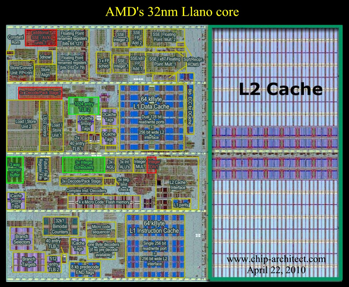
A few observations suggest that AMD's Llano could do AVX instructions.
1) A reasonably large new block next to the FP register file.
2) Something what could be a new 3-way extra decoding stage in front of the FP units.
3) The large increase in size of the reorder buffer (3x24 to 3x32 or 3x36)
-It would be faster even if it's still using 128 bit hardware for the 256 bit
operations since typically many time slots are unused in FP units.
-The AVX performance would be ultimately limited by the cache bandwidth
to/from the SSE/AVX units (32 byte/cycle versus 48 byte/cycle for Sandy
Bridge)
-The 256 bit operations would be split into independent 128 bit operations
which would explain the increase in size of the reorder buffer.
-The size of the 3-way decode pack stage in front of the Integer units
has also increased also suggesting that something is added to the
decoding units (cache access for 2x128 bit words?)
------------------------------
Some extra points:
The second level TLB units for the data cache have been doubled from
512 entries to 1024 entries.
There is extra integer logic. A good guess would be a faster version
of the Integer divider. One that can produce multiple result bits/cycle
like the ones in the Core2 and Nehalem architecture.
Regards, Hans

 Reply With Quote


Bookmarks