


Lol sorry for quoting myself here but this is the perfect example of what I once mentioned on a different day in this topic.Originally Posted by NaMcO

Nvidia has a real tight hold on some of its old school customers..
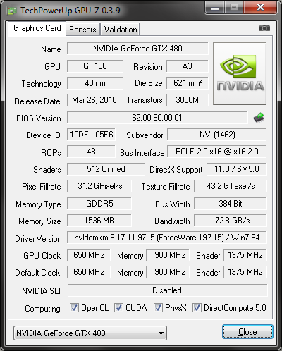
http://www.xtremesystems.org/forums/...82#post4254282


 There has always been a growing peroid with new APIs and their respective hardware. By the time we have enough DX11 games to care about, we should have adequete hardware to handle them. As it stands the very small amount of titles isn't reason enough. Buy a HD5 series or GT4xx because of performance in current (DX9/10) games.

Bookmarks