Quote Originally Posted by sakis_the_fraud View Post
i have posted this before the backup came up, i will write it again.

my goal is to make mobo stable at 530x8 (or 8,5 if that's possible! 
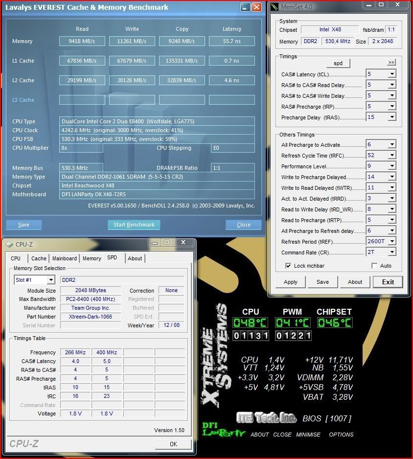
). I own an 8400 and a 2x2 kit, temgroup Xtreem, max memtest on this mobo 550 .

i managed to boot at these settings:


Code:
CPU Feature
- Thermal Management Control: Disabled
-  PPM(EIST) Mode: Disabled
- Limit CPUID MaxVal: Disabled
- CIE Function: Disabled
- Virtualization Technology: Disabled
- Core Multi-Processing: Enabled

Exist Setup Shutdown: Mode 2
O.C. Fail retry Counter: 1
O.C. Fail CMOS Reload: Disabled
CPU Clock Ratio: 8x
CPU N/2 Ratio: Disabled
Target CPU Clock: 4240Mhz
CPU Clock: 530
Boot Up Clock: AUTO
CPU Clock Amplitude: 800mv
CPU Clock0 Skew: 200ps
CPU Clock1 Skew: 0ps
DRAM Speed: 333/667
- Target DRAM Speed: DDR2-667
PCIE Clock: 100mhz

CPU Spread Spectrum: Disabled
PCIE Spread Spectrum: Disabled

Voltage Settings
CPU VID Special Add: +325mv
DRAM Voltage Control: 2.30v
SB Core/CPU PLL Voltage: 1.51
NB Core Voltage: 1.55
CPU VTT Voltage: 1.250
Vcore Droop Control: Enabled
Clockgen Voltage Control: 3.45v
GTL+ Buffers Strength: Strong
Host Slew Rate: strong
x MCH RON Offset Value:00
x MCH RTT Offset Value:00
x MCH Slew Rate Offset Value:00
x MCH VREF 1 Value:23
x MCH VREF 2 Value:23
x MCH VREF 3 Value:A3
x CPU GTL 0/2 REF Volt: 0.620X
x CPU GTL 1/3 REF Volt: 0.620X
x North Bridge GTL REF Volt: 0.67X

DRAM Timing
- Enhance Data transmitting: AUTO
- Enhance Addressing: AUTO
- T2 Dispatch: Disabled

Clock Setting Fine Delay
- DRAM CLK Driving Strength: Level 5
- DRAM DATA Driving Strength: Level 8
- Ch1 DLL Default Skew Model: Model 3
- Ch2 DLL Default Skew Model: Model 3

Fine Delay Step Degree: 5ps to 80ps

Ch1 Clock Crossing Setting: AUTO
- DIMM 1 Clock fine delay: Current 2024ps
- DIMM 2 Clock fine delay: Curren 1174ps
- DIMM 2 Control fine delay: Current 1112ps
- DIMM 1 Control fine delay: Current 1112ps
- Ch 1 Command fine delay: Current 74ps

Ch2 Clock Crossing Setting: AUTO
- DIMM 3 Clock fine delay: Current 1900ps
- DIMM 4 Clock fine delay: Current 937ps
- DIMM 4 Control fine delay: Current 886ps
- DIMM 3 Control fine delay: Current 224ps
- Ch 2 Command fine delay: Current 280ps

Ch1Ch2 CommonClock Setting: AUTO

Ch1 RDCAS GNT-Chip Delay: Auto
Ch1 WRCAS GNT-Chip Delay: Auto
Ch1 Command to CS Delay: Auto

Ch2 RDCAS GNT-Chip Delay: Auto
Ch2 WRCAS GNT-Chip Delay: Auto
Ch2 Command to CS Delay: Auto

Common CMD to CS Timing: 1N/2N/AUTO (command rate)

CAS Latency Time (tCL): 5
RAS# to CAS# Delay (tRCD): 5
RAS# Precharge (tRP): 5
Precharge Delay (tRAS): 15
All Precharge to Act: AUTO
REF to ACT Delay (tRFC): AUTO
Performance LVL (Read Delay) (tRD): AUTO

Read delay phase adjust: Enter

Ch1 Read delay phase (4~0)
- Channel 1 Phase 0 Pull-In: AUTO
- Channel 1 Phase 1 Pull-In: AUTO
- Channel 1 Phase 2 Pull-In: AUTO
- Channel 1 Phase 3 Pull-In: AUTO
- Channel 1 Phase 4 Pull-In: AUTO

Ch2 Read delay phase (4~0)
- Channel 2 Phase 0 Pull-In: Auto
- Channel 2 Phase 1 Pull-In: Auto
- Channel 2 Phase 2 Pull-In: Auto
- Channel 2 Phase 3 Pull-In: Auto
- Channel 2 Phase 4 Pull-In: Auto

MCH ODT Latency: AUTO
Write to PRE Delay (tWR): AUTO
Rank Write to Read (tWTR): AUTO
ACT to ACT Delay (tRRD): AUTO
Read to Write Delay (tRDWR): AUTO
Ranks Write to Write (tWRWR): AUTO
Ranks Read to Read (tRDRD): AUTO
Ranks Write to Read (tWRRD): AUTO
Read CAS# Precharge (tRTP): AUTO
ALL PRE to Refresh: AUTO
used some settings from there -> http://www.outofspecs.gr/forum/showt...?t=2252&page=2

i managed to boot at my desired settings but it isn't stable.

also, i don't know how do we set the MCH VREFs and the driving strength. if there is a guide or something it would be appreciated.
Driving strength is set for the ICs. 6/8 usually works by default. To adjust you either increase clk drive/decrease dq drive or decrease clk drive/increase dq drive, but you need to change DLL models too when doing this.

On my DDR2 G.Skill 1100mhz 2x2gb sticks I've found the best combo for me is, in the format CK Drv/DQ Drv/Dll 1/Dll 2

3/8/5/5 or 4/7/6/6.

Drive strength is the amplitude the clock out and data out are driven at within the DDR delay locked loop relevant to clock in, and out for ddr mux.

MCH Vref are set with respect to the difference default.

Vref1=00h, Vref2=00h, Vref3=80h.

The represent voltage reference points at voltage crossing. You adjust them to the same ratio they are set. ie, Vref1=05h, Vref2=05h, Vref3=85h.

Unless you understand what they do stick to this. Also you can benefit from adjusting MCH slew rate offset, and MCH ROn/Rtt.

Ie.

MCH Rtt = 06h, MCH ROn = 03h, MCH Slew rate = 0Ah, MCH Vref1 = 18h, MCH Vref2 = 18h, MCH Vref3 = 98h

I'm pretty certain that Rtt = 1/2 ROn when setting it, since Rtt is usually 2 * ROn impedance. ie Rtt = 120 ohms, Ron = 60 ohms.