

Stop teasing us with ya mad rams ! but really Everest shows awesome bandwith etc but this is hardly reflected in eg Superpi32... I take everest with a BIG grain of salt !


Stop teasing us with ya mad rams ! but really Everest shows awesome bandwith etc but this is hardly reflected in eg Superpi32... I take everest with a BIG grain of salt !
Question : Why do some overclockers switch into d*ckmode when money is involved
Remark : They call me Pro AsusSaaya yupp, I agree
Hehe sorry about that!
Yes Everest is just synthetic, it's nice for a quick demo but I also prefer something real like 32M to show performance. In my experience the M2F just can't pass SPI32M over 534 FSB / 640 MHz PL8. I have a feeling the MCH is at it's limit around there.
Ci7 990X::Rampage III Extreme::12GB Corsair Dominator 1866C7GT::2 x EVGA SC Titans in SLI::Corsair AX1200::TJ07::Watercooled
Ci7 920 3849B018::Rampage II Extreme::6GB GSKILL Trident 2000C9 BBSE::EVGA GTX580::Antec Signature SG850::TJ09::Aircooled w/TRUE 120X
I'm fighting the P45 UD3P at the moment mate, stuck there at 570FSB Hyperpi 32Mb stable, 575 always gives me one error after each pass, tried zillions of combinations (volts, GTL's, PL's, timings,... ), other rams etc... think it's the limit of my board's chipset... it has to end somewhere lol
Question : Why do some overclockers switch into d*ckmode when money is involved
Remark : They call me Pro Asus
Yeah its tricky sometimes to make it pass, I assume that's on 1:1? I can get 550 FSB 1:1 PL 10 to pass but over that it falls part rapidly, same on my P5Q-Deluxe. Skews really helped me with stability, delay 150ps on each channel was the optimal setting at 534 - 542 FSB & 640 - 651 MHz ram with PL 8.
Ci7 990X::Rampage III Extreme::12GB Corsair Dominator 1866C7GT::2 x EVGA SC Titans in SLI::Corsair AX1200::TJ07::Watercooled
Ci7 920 3849B018::Rampage II Extreme::6GB GSKILL Trident 2000C9 BBSE::EVGA GTX580::Antec Signature SG850::TJ09::Aircooled w/TRUE 120X
Ok, so Quad cores and the MIIF board don't mix. What CPU are you using to achieve these high FSB's??? 8600??? I figure if I'm going to keep this board I might as well, get a CPU that I can have fun with. 480fsb with a quad is nice but 600+++ would be like heaven!
Simonix is usiing an 8600 see his valid link: Here
Ci7 990X::Rampage III Extreme::12GB Corsair Dominator 1866C7GT::2 x EVGA SC Titans in SLI::Corsair AX1200::TJ07::Watercooled
Ci7 920 3849B018::Rampage II Extreme::6GB GSKILL Trident 2000C9 BBSE::EVGA GTX580::Antec Signature SG850::TJ09::Aircooled w/TRUE 120X
Can't you just lower the PL on MIIF directly? I would assume that having the options separate would be more advantageous.Originally Posted by Grnfinger

Or is it that the Phase Pull-Ins on the X38 allowed you to run a lower PL that would not run otherwise?
ES Q9550 E0 @ 4.0GHz (471x8.5) 1.256v
TR-Ultra-120-X, 115CFM 120mm fan
Maximus II Formula @ 1884MHz FSB
Ballistix DDR2-800 (4x1GB) 1132MHz 5-5-5-5-15 4-55-8-14-11-3-8-5-4-2T
eVGA GTX 280 @ 702c/1404s/1260m (1.175v)
Auzentech XPlosion DTS-Interactive Vantage 'X'-6,727
300GB Velociraptor, PC P&C 750W
(3)120mm, (2)90mm, (1)250mm case fans in TT Armor
27.5" LCD/Z-5500-office, 95" 720P projector/7.1ch-living room
Logitech Driving Force Pro-Microsim Racing Pod
The MIIF does fine w/ quads, and for 24/7 you aren't going to get much higher clocks from a dual than a quad (4.2-4.4GHz vs 4.0-4.2GHz). So, ~200Mhz higher w/ the duals, but half the cores.
If you're just talking about benching then yes, the duals can be a lot more fun. You can get near the same results w/ an E8400 E0 as you can w/ the E8600, though, unless you get some extreme cooling. The E8400 has a 9x multi, and if you can get 600FSB then that puts you at 5.4GHz. You're well into extreme cooling at that speed, and the extra multi wouldn't be any good for anything else.
The main thing you want to do if you're shopping for a good dual to play w/ is to try and get a really good batch from somebody. A used chip that is a proven good OCer, or perhaps go to a store that lets you sift through the boxes to find a good batch. It doesn't matter if it's an E0 E8400, E8500, or E8600 as long as you get a really good batch.
ES Q9550 E0 @ 4.0GHz (471x8.5) 1.256v
TR-Ultra-120-X, 115CFM 120mm fan
Maximus II Formula @ 1884MHz FSB
Ballistix DDR2-800 (4x1GB) 1132MHz 5-5-5-5-15 4-55-8-14-11-3-8-5-4-2T
eVGA GTX 280 @ 702c/1404s/1260m (1.175v)
Auzentech XPlosion DTS-Interactive Vantage 'X'-6,727
300GB Velociraptor, PC P&C 750W
(3)120mm, (2)90mm, (1)250mm case fans in TT Armor
27.5" LCD/Z-5500-office, 95" 720P projector/7.1ch-living room
Logitech Driving Force Pro-Microsim Racing Pod
The board is under a EK Supreme, 320, 355, 1/2id... will water be enough for 5.4Ghz 24/7 stable?


Correct
I think you'll need DI or LN2 for that speed, and it wouldn't be 24/7 in any case. All these high FSB speeds you're seeing are not 24/7 stable. I haven't done a lot of duallie super-high FSB 24/7 testing, but I'd say 533 would be getting near the limit for 24/7 stability. Maybe 550-575 if you're lucky. But then you can't run anything but a 1:1 divider, and have to settle for a looser PL.
9x500 w/ 5:6 divider and PL=8 Stronger is a good goal to reach for.
Gotcha. Makes a lot more sense now.
Someone mentioned how the PL levels on the P45 were 1 number higher for the same value on P35/X38/X48. So, PL=7 on X38 is the same as PL=8 on P45. That being said, I was able to hit PL=6 at similar RAM speeds on my P35 P5K-Premium, and have to use PL=8 on my MIIF. Didn't need pull-ins to do it, but the 90nm chipset boards definitely had an advantage w/ bandwidth.
ES Q9550 E0 @ 4.0GHz (471x8.5) 1.256v
TR-Ultra-120-X, 115CFM 120mm fan
Maximus II Formula @ 1884MHz FSB
Ballistix DDR2-800 (4x1GB) 1132MHz 5-5-5-5-15 4-55-8-14-11-3-8-5-4-2T
eVGA GTX 280 @ 702c/1404s/1260m (1.175v)
Auzentech XPlosion DTS-Interactive Vantage 'X'-6,727
300GB Velociraptor, PC P&C 750W
(3)120mm, (2)90mm, (1)250mm case fans in TT Armor
27.5" LCD/Z-5500-office, 95" 720P projector/7.1ch-living room
Logitech Driving Force Pro-Microsim Racing Pod
guys i need to change dissipation system on my M2F..ni got really nice results but NB temp are too high..i could even go on in OC if i reduce my temps..
what aftermarket cooler could i use for SB and NB ?
noctua NC U6 fit into NB without hurts ram slots ? no problem for Sb i think, even blue ice cooler is sufficient for SB.
i have even seen extreme sprit 2 by thermaltake that is smaller but i don't know if it's able to dissipate well.. i want to replace all pipes on my board ..i'm 55 °C on NB in idle
Maximus III Formula - i7 860 4Ghz - 4 GB Gskill Ripjaws 2Ghz - Powercolor 5850 1000/1250 VF3000A - XFI Titanium Fatality - WD3200AAKS RAID 0 - Maxtor 500 Gb - Wd 5000AAKS - Enermax 625W modu82+ - Case CM690 - CM TX3
Exteme spirit works well and is a cost effective soloution alittle noisey tho if you dont run it on a fan controller.
Vantec icberq copper cooler works very well with slight mod to mounting holes and looks nice
Cannot comment on the noctua, but I do recall someone posting that it works but not sure if it was this board or not..
So, I've been running stability tests on my MIIF, Q9650, & DDR2 1000 - I was having trouble completing SuperPI and HyperPI but it was stable for 12hrs blend on Prime95 @ 480fsb ... I thought it was ok. I recently tried IBT & it failed. I reset my bios and all settings go default and it still fails IBT I am currently running HCI memtest to recheck ram. I was running 1.43v on the core to run the 480fsb (8.5multi) - could the CPU be failing or the mobo?
EDIT: How about an E8600 for this board? I've decided to run my other quad with my UD3R board. What fsb could I expect with an E8600 in a 24/7 scenario? Also heard there is an E8700 coming out, any idea when or is it bs?
Last edited by 529th; 03-22-2009 at 11:20 AM.
8700 is due out soon I think..
To switch from a quad to a dualie I think you will regret it.
I have a 8400 on my second MIIF and its a dog compared to the 4.2GHz Q9650.
480fsb is very doable on this board, It took me 20 mins maybe to dial in my 4.2GHz settings, all my chips will do 500FSB on this board.
I would recheck your settings
This is my 4200MHz setup
Extreme Tweaker
Ai Overclock Tuner : Manual
OC From CPU Level Up : AUTO
CPU Ratio Control : Manual
- Ratio CMOS Setting : 9
FSB Frequency : 467
CPU Clock Skew : Advanced 100ps
North Bridge Clock Skew : Advanced 100ps
FSB Strap to North Bridge : 333
DRAM Frequency: DDR2-1121
Dram Clock Skew CH1 A1 : Normal
DRAM Clock Skew CH1 A2 : Normal
Dram Clock Skew CH1 B1 : Normal
Dram Clock Skew CH1 B2 : Normal
DRAM Timing Control: Manual
CAS# Latency : 5
RAS# to CAS# Delay : 5
RAS# Precharge : 5
RAS# ActivateTime : 15
RAS# to RAS# Delay : 3
Row Refresh Cycle Time : 55
Write Recovery Time : 6
Read to Precharge Time : 3
Read to Write Delay (S/D) : 8
Write to Read Delay (S) : 3
Write to Read Delay (D) : 5
Read to Read Delay (S) : 4
Read to Read Delay (D) : 6
Write to Write Delay (S) : 4
Write to Write Delay (D) : 6
Write to PRE Delay : 14
Read to PRE Delay : 5
PRE to PRE Delay : 1
ALL PRE to ACT Delay : 5
ALL PRE to REF Delay : 5
DRAM Static Read Control: Enabled
Dram Read Training : Disabled
MEM OC Charger : Enabled
Ai Clock Twister : Stronger
Transaction Booster : Manual
Common Performance Level [8]
Pull-In of CHA PH1 Disabled
Pull-In of CHA PH2 Disabled
Pull-In of CHA PH3 Disabled
Pull-In of CHA PH4 Disabled
Pull-In of CHA PH5 Disabled
Pull-In of CHB PH1 Disabled
Pull-In of CHB PH2 Disabled
Pull-In of CHB PH3 Disabled
Pull-In of CHB PH4 Disabled
Pull-In of CHB PH5 Disabled
PCIE Frequency : 103
CPU Voltage : 1.325
CPU PLL Voltage : 1.59275
FSBT : 1.37825
DRAM Voltage : 1.9
North Bridge Voltage : 1.45775
South Bridge Voltage 1.5 : 1.55300
South Bridge Voltage 1.1 : 1.20600
CPU GTL Reference 0 : Auto
CPU GTL Reference 1 : -45mv
CPU GTL Reference 2 : Auto
CPU GTL Reference 3 : -45mv
North Bridge GTL Reference : AUTO
DDR2 Channel A REF Voltage : AUTO
DDR2 Channel B REF Voltage : AUTO
North Bridge DDR Reference : AUTO
Load Line Calabration : Enabled
CPU Sread Spectrum : Disabled
PCIE Spread Spectrum : Disabled
That all seems to be working except for my memory sub timings are on auto and I have to use PL 10 with the DDR2 1000 I am running 1:1 btw
I am testing currently using Prime95 blend, then I'm going to test with IBT - I've never seen what you have for results with your IBT screenie, what did you do? btw, my system will not pass the "max stress" test under IBT
EDIT: ah poop, failed both Prime blend & OCCT - upping vcore to 1.38 vtt to 1.37
Last edited by 529th; 03-22-2009 at 04:36 PM.
Eh, the E8600 will not be the highest clocking Wolfdale ever binned?
heard the E8600 was the last


Thats mine :

Intel Q9650 @500x9MHz/1,3V
Asus Maximus II Formula @Performance Level=7
OCZ OCZ2B1200LV4GK 4x2GB @1200MHz/5-5-5-15/1,8V
OCZ SSD Vertex 3 120Gb
Seagate RAID0 2x ST1000DM003
XFX HD7970 3GB @1111MHz
Thermaltake Xaser VI BWS
Seasonic Platinum SS-1000XP
M-Audio Audiophile 192
LG W2486L
Liquid Cooling System :
ThermoChill PA120.3 + Coolgate 4x120
Swiftech Apogee XT, Swiftech MCW-NBMAX Northbridge
Watercool HeatKiller GPU-X3 79X0 Ni-Bl + HeatKiller GPU Backplate 79X0
Laing 12V DDC-1Plus with XSPC Laing DDC Reservoir Top
3x Scythe S-FLEX "F", 4x Scythe Gentle Typhoon "15", Scythe Kaze Master Ace 5,25''
Apple MacBook Pro 17` Early 2011:
CPU: Sandy Bridge Intel Core i7 2720QM
RAM: Crucial 2x4GB DDR3 1333
SSD: Samsung 840 Pro 256 GB SSD
HDD: ADATA Nobility NH13 1GB White
OS: Mac OS X Mavericks
When they read this Intel sees $$$
So hence the 8700
8700? i know that Fugger has told that isn't confirmed ...
OBSIDIAN 800D, ASRock P67 Professional, Intel 2600K [UNLOCKED] watercooled by Ybris Black Sun (HWLabs Black Ice SR1-360 w/Nanoxia 2K, Swiftech MCP655 + Res XSPC), 4GB KINGSTON LoVo, SSD 128GB Crucial RealSSD C300, HDD Seagate Barracuda 250GB/500GB, Corsair HX 750w, nVidia 260 GTX XFX Black Edition, X-FI Xtreme Gamer
8700, wow! Didn`t know !
Intel Q9650 @500x9MHz/1,3V
Asus Maximus II Formula @Performance Level=7
OCZ OCZ2B1200LV4GK 4x2GB @1200MHz/5-5-5-15/1,8V
OCZ SSD Vertex 3 120Gb
Seagate RAID0 2x ST1000DM003
XFX HD7970 3GB @1111MHz
Thermaltake Xaser VI BWS
Seasonic Platinum SS-1000XP
M-Audio Audiophile 192
LG W2486L
Liquid Cooling System :
ThermoChill PA120.3 + Coolgate 4x120
Swiftech Apogee XT, Swiftech MCW-NBMAX Northbridge
Watercool HeatKiller GPU-X3 79X0 Ni-Bl + HeatKiller GPU Backplate 79X0
Laing 12V DDC-1Plus with XSPC Laing DDC Reservoir Top
3x Scythe S-FLEX "F", 4x Scythe Gentle Typhoon "15", Scythe Kaze Master Ace 5,25''
Apple MacBook Pro 17` Early 2011:
CPU: Sandy Bridge Intel Core i7 2720QM
RAM: Crucial 2x4GB DDR3 1333
SSD: Samsung 840 Pro 256 GB SSD
HDD: ADATA Nobility NH13 1GB White
OS: Mac OS X Mavericks
Is that a joke ? So take a look at this mates
http://www.hwbot.org/quickSearch.do?...+(3.50Ghz)+(0)
This page is mine
Klan-OC Team .fr
- ASUS M5G/M4G - GIGABYTE GA-P55/67A-UD7 - EVGA P55 FTW - GA-EP45-UD3P -
- INTEL i7 3770 & 2600K/i5 750/i5 661 & i3 530/E8600/E6800/E6500K +CORSAIR H70 or THERMALRIGHT TrueBlack 120 (Full WC/SS/Cascade/LN² optional ^^) -
- G.SKILL TridentX PC3 2400C10 (2x4gb)/Ripjaws X PC3 17600C7 & PerfectStorm PC3 17066C8[/B] (2x2gb)/CRUCIAL Value PC3 10700 (2x1gb @880 cas6)
CRUCIAL BallistiX Tracer PC8500 (2x1gb @704 cas5) -
- SAPPHIRE HD 7970 / SLI MSI GTX580 Lightning / MSI GTX275 Lightning / MSI GTX 560Ti Hawk / ASUS HD 4870 1Gb DK / CFs MSI HD5770 Hawk & ASUS HD4770 -
- CORSAIR AX1200 & HX650 / ENERMAX REVOLUTION 1250w & MODU 82+625w -
- CRUCIAL M4 128Gb RAID0 /OCZ Vertex 3 120Gb & Turbo 30Gb / WD Velociraptor 150Gb/Raid0 & WD Raptor 76Gb/Raid0 /3x WD Caviar Black 2To -

THE AMOUNT OF HW ISN'T REPRESENTATIVE OF YOUR SKILLZ ...IF YOU'RE THE KING OF THE HILL, PROVE IT THOUGH!!
thank you for reply, i probably go for extreme spitir so it's compatible without mods..i think oi can set 60% of speed from bios if it will be noisy, it's active dissipation so it's sufficenti'll post the mod as soon as i do

Maximus III Formula - i7 860 4Ghz - 4 GB Gskill Ripjaws 2Ghz - Powercolor 5850 1000/1250 VF3000A - XFI Titanium Fatality - WD3200AAKS RAID 0 - Maxtor 500 Gb - Wd 5000AAKS - Enermax 625W modu82+ - Case CM690 - CM TX3
Shops in Europe are taking orders for E8700 now.
As far as I know there going to be released as Intel has not stated when 775 will be EOL
i7 is still in its infancy and i5 has not seen retail yet, so I cant see Intel dropping 775 yet.
select no to "turn on error dection" and you will get the same output
What test are you failing in Prime?
Please post back with your results
Last edited by Grnfinger; 03-23-2009 at 02:12 PM.
That's old news m8.
The I7 is not selling as well as they would like and I5 is belated and the World Wide Recession does not help.
Even before this they said I7 would not be mainstream even for high end segment till late 2009/early 2010.
There is a E8700 due and their is a few new socket 775 Mobos with DDR2 1333mhz support out/due out soon.
I also say there will be a new 45nm Quad out faster than the Q6950 but that's IMO.
I did foresee the new "S Model" 65watt 45nm Quads.


 Reply With Quote
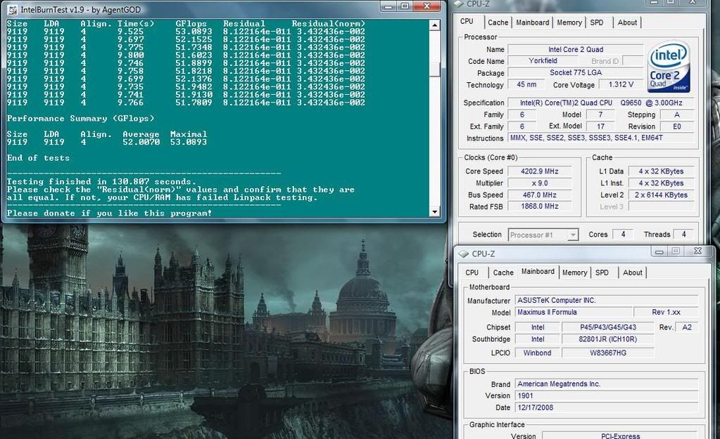


Bookmarks