


I have been playing with BIOS 913 & found it makes a tad more bandwidth with slightly better latency at the expense of a tad more vNB & vDIMM.
The 913 BIOS also benches realy well IMO, I have had tons of fun & seen some awesome numbers from it.
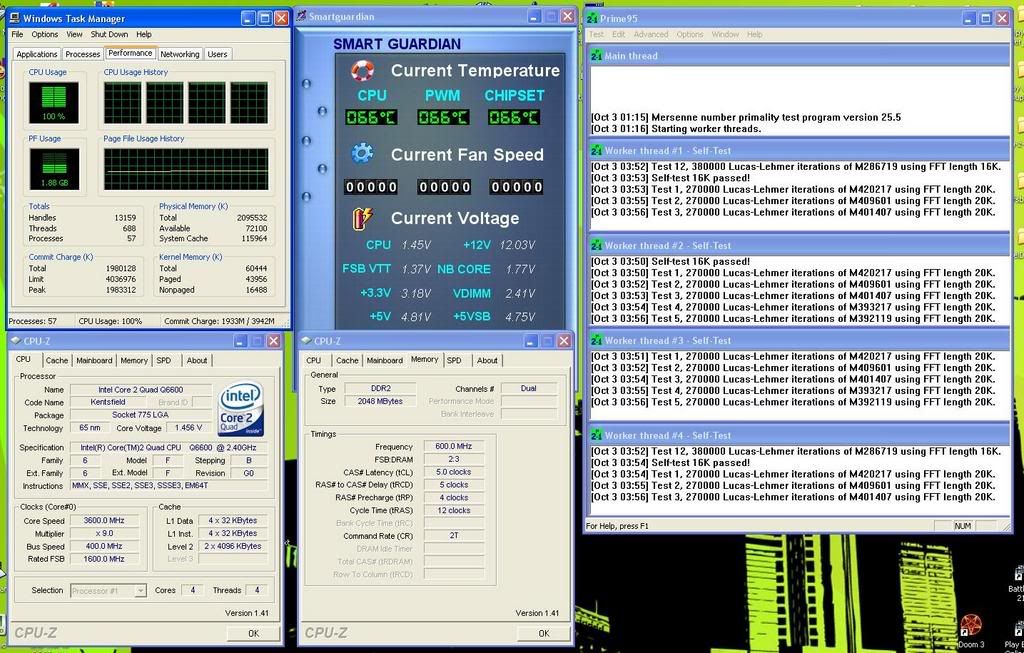
Here is my rigs sweet spot with the 913 BIOS.
==================================
DFI LANPARTY UT P35-T2R (BIOS 913)
INTEL CORE 2 DUO QUAD Q6600 KENTSFIELD 2.4GHZ 4M L2 CACHE
OCZ PC2-8500 SLI 2 x 1GB PN:OCZN1066SR2GK
INNO3D 8800GTS 320MB (162.18 DRIVERS + OVERCLOCK 617 X 955)
4 X HITACHI DJ 80GB HD'S (RAID 0 / 64K STRIPE)
SONY DUAL LAYER DVD RW (DRU-820A)
OCZ GAMEXTREAM 1010W PSU
WINDOWS XP PRO SP2
CPU COOLING: THERMALRIGHT ULTRA-120 EXTREME
PRIME95 + 3DMARK2001SE + 3x CPU-Z:(SCORE 63,338)Code:>CPU Feature: Thermal Management Control.......... - Disabled PPM(EIST) Mode...................... - Disabled Limit CPUID MaxVal.................. - Disabled CIE Function........................ - Disabled Execute Disable Bit................. - Enabled Virtualization Technology........... - Enabled Core Multi-Processing............... - Enabled >DRAM Timing: Enhance Data transmitting........... - Fast Enhance Addressing.................. - Fast T2 Dispatch......................... - Disabled >Clock Setting Fine Delay Press Enter: Ch1 Clock Crossing Setting......... - More Aggressive DIMM1 Clock Fine Delay............. - Current[1] DIMM2 Clock Fine Delay............. - Current[6] Ch1 ControlFine Delay.............. - Current[9] Ch1 ControlFine Delay.............. - Current[6] Ch2 Clock Crossing Setting......... - More Aggressive DIMM3 Clock Fine Delay............. - Current[1] DIMM4 Clock Fine Delay............. - Current[6] Ch2 ControlFine Delay.............. - Current[9] Ch2 ControlFine Delay.............. - Current[6] Ch1 Ch2 Common Clock Setting....... - More Aggressive Ch1 RDCAS GNT-Chip Delay........... - Auto Ch1 WRCAS GNT-Chip Delay........... - Auto Ch1 Command To CS Delay............ - Auto Ch2 RDCAS GNT-Chip Delay........... - Auto Ch2 WRCAS GNT-Chip Delay........... - Auto Ch2 Command To CS Delay............ - Auto CAS Latency Time (tCL).............. - 5 RAS# to CAS# Delay (tRCD)........... - 5 RAS# Precharge (tRP)................ - 5 Precharge Delay (tRAS).............. - 15 All Precharge to Act................ - 5 REF to ACT Delay (tRFC)............. - 30 Performance Level................... - 7 >Read delay phase adjust Press Enter: Channel 1 Phase 0 Pull-In.......... - Auto Channel 1 Phase 1 Pull-In.......... - Auto Channel 1 Phase 2 Pull-In.......... - Auto Channel 1 Phase 3 Pull-In.......... - Auto Channel 1 Phase 4 Pull-In.......... - Auto Channel 2 Phase 0 Pull-In.......... - Auto Channel 2 Phase 1 Pull-In.......... - Auto Channel 2 Phase 2 Pull-In.......... - Auto Channel 2 Phase 3 Pull-In.......... - Auto Channel 2 Phase 4 Pull-In.......... - Auto MCH ODT Latency..................... - Auto Write to PRE Delay (tWR)............ - 13 Rank Write to Read (tWTR)........... - 11 ACT to ACT Delay (tRRD)............. - 3 Read to Write Delay (tRDWR)......... - 8 Ranks Write to Write (tWRWR)........ - Auto Ranks Read to Read (tRDRD).......... - Auto Ranks Write to Read (tWRRD)......... - Auto Read CAS# Precharge (tRTP).......... - 4 ALL PRE to Refresh.................. - 5 >Voltage Settings: CPU VID Control..................... - 1.52500v CPU VID Special Add................. - Auto DRAM Voltage Control................ - 2.35v SB 1.05V Voltage.................... - 1.070v SB Core/CPU PLL Voltage............. - 1.55v NB Core Voltage..................... - 1.61v CPU VTT Voltage..................... - 1.60v Vcore Droop Control................. - Disabled Clockgen Voltage Control............ - 3.45v GTL+ Buffers Strength............... - Weak Host Slew Rate...................... - Weak GTL REF Voltage Control............. - Disable CPU GTL1/3 REF Volt................. - 115 CPU GTL 0/2 REF Volt................ - 115 North Bridge GTL REF Volt........... - 115 Genie BIOS Settings: Exist Setup Shutdown................ - Mode 2 CLOCK VC0 divider................... - Auto CPU Clock Ratio Unlock.............. - Enabled CPU Clock Ratio..................... - 8 Target CPU Clock.................... - 3800MHz CPU Clock........................... - 475 Boot Up Clock....................... - 265 DRAM Speed.......................... - 333/800 Target DRAM Speed................... - 1141MHz PCIE Clock.......................... - 110mhz PCIE Slot Config.................... - 1X 1X CPU Spread Spectrum................. - Disabled PCIE Spread Spectrum................ - Disabled SATA Spread Spectrum................ - Disabled
http://i106.photobucket.com/albums/m...Hz3DMARK01.jpg
3DMARK2003:(SCORE 38,156)
http://i106.photobucket.com/albums/m...Hz3DMARK03.jpg
3DMARK2005:(SCORE 19,881)
http://i106.photobucket.com/albums/m...Hz3DMARK05.jpg
3DMARK2006:(SCORE 12,123)
http://i106.photobucket.com/albums/m...Hz3DMARK06.jpg
AQUAMARK 3:(SCORE 209,326)
http://i106.photobucket.com/albums/m...3/Aquamark.jpg
SHORT DESCRIPTION:
475 x 8 = 3.8GHZ @ 1.5250v
5-5-5-15 2T @ 2.350V DDR 1141
=================================
I have attached the template I used above if anyone wants to use it be my guest.
CN.


 Reply With Quote


 i7 920@2.8
  X3220@3.0
 X3220@2.4
  E8400@4.05
  E6600@2.4


 I just received it in the Mail Today


Bookmarks