


Instead of cluttering up another thread i decided to make one so here goes.....
OK first we need a picture of a cpu........Particle I used yours again I hope you don't mind
Photo courtesy of particle as long as he lets me use it.
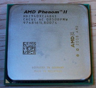
So here we have a typical 940 CPU
Lets start with the 5 digit code CACVC
First letter is the production/release code if this was an ES chip it would be an A. They are using the letter C for current production release chips although they don't always use C
2nd letter is the Core Cache code It will probably be different with lets say X3chips and X2's with less cache
3rd and 4th letter identify the memory controller revision. This apparently is a CV revision memory controller.
5th letter is usually a revision code
C = Deneb most likely in this case......
Next we move onto the 4 digit number code......
year and week
The chip pictured appears to be made in 08 week 50 so around december 14th...
Now the last 4 has always been vague but i've always believed them to be the code that determined who tested, time of day, etc etc.....I really don't think its as pertinent unless the guy testing was half in the bag (not likely)
Now to the bottom of the chip.
Last 6
L I think ( it's been a while ) means Lot as in Lot # ****CORRECTION**** the letter before th batch is a date code......
the last 5 tell you what batch it came from and what # it was in the batch ****Correction**** the 8 in this case means 2008
This is batch 80000 which will probably go up to 81000 and this particular chip was # 74 out of 1000.
Anyway this concludes my lesson on stepping and batch numbers for now....more to follow in the future......
****EDIT**** the purpose of the lower line for AMD is it's a serial # for them to specifically ID a chip...whether for RMA purposes or to keep track of chips not specified for retail or other reasons unbeknown at this time.


 Reply With Quote

 Particle's First Rule of Online Technical Discussion:
 Rule 1A:
 Rule 2:
 Rule 2A:
 Rule 3:


 I just wonder who said that that pair of letters identifies the memory controller for the first time, it would be nice to see the reason behind that conclusion. Just note that there are chips from the 754 era (130nm) that, if this is correct, have AA memory controllers. Also note that thereare 9850BE's with that "memory controller" as well. There are also alot of similar memory controllers bewteen 939 and AM2 (like BA, BB, B9, BU(?), BF, BG)


Bookmarks