MMM
Results 1 to 25 of 82

Thread: AMD talks up its first Fusion chip

Hybrid View

  1. #1
    Xtreme Member
    Join Date
    Aug 2004
    Posts
    210
    Quote Originally Posted by Hans de Vries View Post
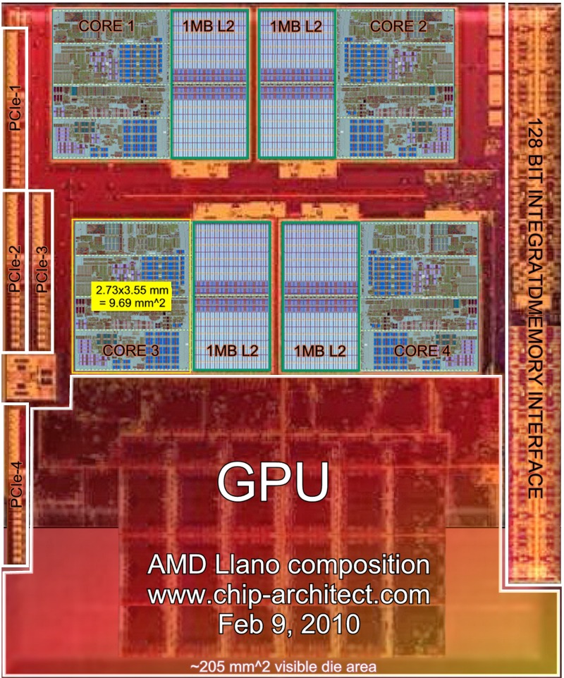
    Later die pictures showed more GPU area so the die for so far is ~205mm^2

    Could you distinguish the HT ports from PCIe Lanes/ports ?
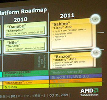
    AMD earlier said that Fusion parts will come with PCIe Gen 2, only. So there should not be any Hypertransport at all.


    There are also no NB chipsets mentioned in the table from above, only a SB part (Hudson).

    Thus the ports that you named HT2 & HT3 are probably PCIe connectors that could be used for a dedicated graphic card (2x x8).
    Another link will be probably used to connect to the southbridge, ATIs ALink is nothing more then a relabeled PCIe.

    The last link could be used for anything else, PCIe x1 Slots, onboard chips, etc.

    Furthermore the square die area below HT2 and HT3 and above HT4: Could that be the PCIe logic ?

    cheers
    Last edited by Opteron146; 02-09-2010 at 08:16 AM.

  2. #2
    Xtreme Member
    Join Date
    Sep 2008
    Posts
    235
    Quote Originally Posted by Opteron146 View Post
    Could you distinguish the HT ports from PCIe Lanes/ports ?
    AMD earlier said that Fusion parts will come with PCIe Gen 2, only. So there should not be any Hypertransport at all.


    There are also no NB chipsets mentioned in the table from above, only a SB part (Hudson).

    Thus the ports that you named HT2 & HT3 are probably PCIe connectors that could be used for a dedicated graphic card (2x x8).
    Another link will be probably used to connect to the southbridge, ATIs ALink is nothing more then a relabeled PCIe.

    The last link could be used for anything else, PCIe x1 Slots, onboard chips, etc.

    Furthermore the square die area below HT2 and HT3 and above HT4: Could that be the PCIe logic ?

    cheers

    You are right Opteron146 according to the presentation.
    The PCIe lanes have moved from the chip-set to the CPU/GPU die.
    The Llano compilation is already updated.


    Regards, Hans

  3. #3
    Xtreme Member
    Join Date
    Jul 2004
    Location
    Berlin
    Posts
    275
    Quote Originally Posted by Hans de Vries View Post
    You are right Opteron146 according to the presentation.
    The PCIe lanes have moved from the chip-set to the CPU/GPU die.
    The Llano compilation is already updated.


    Regards, Hans
    An even higher res Llano shot can be found at
    http://www.pcgameshardware.de/aid,70...fikkarte/News/:

    (Thanks to Opteron@Planet3dnow! for the copy - the same as Opteron146 here?)

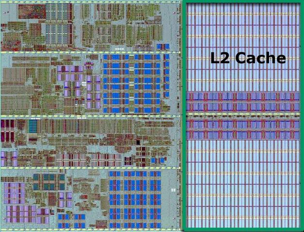
    This might be interesting for core comparisons, for example to find out, what this is (APM? more TLBs? or related to dynamic cache resizing?):

    .
    Now on Twitter: @Dresdenboy!
    Blog: http://citavia.blog.de/

  4. #4
    Xtreme Member
    Join Date
    Aug 2004
    Posts
    210
    Quote Originally Posted by Dresdenboy View Post
    (Thanks to Opteron@Planet3dnow! for the copy - the same as Opteron146 here?)
    Klar, wer sonst

  5. #5
    Xtreme Member
    Join Date
    Sep 2008
    Posts
    235
    Quote Originally Posted by Dresdenboy View Post
    An even higher res Llano shot can be found at
    http://www.pcgameshardware.de/aid,70...fikkarte/News/:

    (Thanks to Opteron@Planet3dnow! for the copy - the same as Opteron146 here?)

    This might be interesting for core comparisons, for example to find out, what this is (APM? more TLBs? or related to dynamic cache resizing?):

    .
    Nice find! There's one slightly bigger version over there:


    Regards, Hans

  6. #6
    Xtreme Member
    Join Date
    Aug 2004
    Posts
    210
    Quote Originally Posted by Hans de Vries View Post
    Nice find! There's one slightly bigger version over there:

    http://www.pcgameshardware.de/screen...o-Vierkern.jpg
    Haha, same error as over @P3D, there is just a small "No Deeplink" message.
    But it seems that I got a downsized picture last time, or PCGH changed the pic in the meantime.

    Anyways, here's the pic:


    @Dresdenboy:
    I'll change it over at P3D, too.
    One idea for the changed area: Maybe some changes in the cache controller, due to the 8T cache cells (K10 had 6T) ?

    cheers

    Alex
    Last edited by Opteron146; 02-09-2010 at 07:05 PM.

  7. #7
    Xtreme Member
    Join Date
    Jul 2004
    Location
    Berlin
    Posts
    275
    Quote Originally Posted by Opteron146 View Post
    @Dresdenboy:
    I'll change it over at P3D, too.
    One idea for the changed area: Maybe some changes in the cache controller, due to the 8T cache cells (K10 had 6T) ?
    BTW, yesterday I looked for any reference to 8T cache cells in the reports and didn't find anything or overlooked it. IIRC, this subtopic has been announced for this ISSCC.
    Now on Twitter: @Dresdenboy!
    Blog: http://citavia.blog.de/

  8. #8
    Xtreme Member
    Join Date
    Aug 2004
    Posts
    210
    Quote Originally Posted by Dresdenboy View Post
    BTW, yesterday I looked for any reference to 8T cache cells in the reports and didn't find anything or overlooked it. IIRC, this subtopic has been announced for this ISSCC.
    Yes, it was mentioned earlier in an eetimes article:
    Much of AMD's paper will focus on circuit techniques the company is using to lower power consumption and leakage of the core. For example, the core's L1 cache uses 8T memory cells to support low supply voltages.
    http://www.eetimes.com/rss/showArtic...leID=221900830

    I guess they just forgot that in the telephone conference. IMO, there are still no real ISSCC articles.

  9. #9
    Xtreme Addict
    Join Date
    Apr 2006
    Posts
    2,462
    Quote Originally Posted by Opteron146 View Post
    @Dresdenboy:
    I'll change it over at P3D, too.
    One idea for the changed area: Maybe some changes in the cache controller, due to the 8T cache cells (K10 had 6T) ?

    cheers

    Alex
    Does 6T mean six transistors per cache cell? So Llano's cache might need more space for the same amount, but on the other hand need less energy?

    P.S. Dann bist du wohl auch der Opteron der im Luxx sein "Unwesen" treibt, was? :P
    Notice any grammar or spelling mistakes? Feel free to correct me! Thanks

  10. #10
    Xtreme Member
    Join Date
    Sep 2008
    Posts
    235
    Quote Originally Posted by FischOderAal View Post
    Does 6T mean six transistors per cache cell? So Llano's cache might need more space for the same amount, but on the other hand need less energy?
    The blocks containing the L1 data and instruction cache are some 10%
    wider relatively compared to the 45nm layout because of the larger 8T
    cells. Intel uses 8T cells for the L1 caches at 32nm at well.

    The extra room is used for the extra logic Mathias was talking about.


    Regards, Hans

  11. #11
    Xtreme Mentor
    Join Date
    Mar 2006
    Posts
    2,978
    Quote Originally Posted by FischOderAal View Post
    Does 6T mean six transistors per cache cell? So Llano's cache might need more space for the same amount, but on the other hand need less energy?

    P.S. Dann bist du wohl auch der Opteron der im Luxx sein "Unwesen" treibt, was? :P
    Yes, 6T stands for 6 transistor, most of the cache in the last several years were based on a 6 transistor bit cell (for storing one bit), Intel implemented an 8T transistor cell in their 45 nm Nehalem, and it appears (interestingly enough) that AMD will do the same.

    Logically, 8T should take up more area, depending on the layout how much more area is not going to be exactly clear unless AMD publishes a cell layout picture.

    It is counter intuitive that 8T should consume less power than 6T, and all things being equal it 8T would consume more power than 6T. However, 8T allows voltage to be dropped (not as sensitive to lower voltage limit) in lower power standby, which has a net win on power.
    One hundred years from now It won't matter
    What kind of car I drove What kind of house I lived in
    How much money I had in the bank Nor what my cloths looked like.... But The world may be a little better Because, I was important In the life of a child.
    -- from "Within My Power" by Forest Witcraft

  12. #12
    Registered User
    Join Date
    Feb 2010
    Location
    Poland
    Posts
    6
    Quote Originally Posted by Dresdenboy View Post
    An even higher res Llano shot can be found at
    This might be interesting for core comparisons, for example to find out, what this is (APM? more TLBs? or related to dynamic cache resizing?):

    .
    I see more changes:

    Longer Shedulers or ALU/AGUs ??
    Increased reorder buffer ??
    New unit next to the FPU register?? (currently it is empty space)


  13. #13
    Xtreme Member
    Join Date
    Aug 2004
    Posts
    210
    Quote Originally Posted by Zibi View Post
    I see more changes:

    Longer Shedulers or ALU/AGUs ??
    Increased reorder buffer ??
    Yes, this is mentioned in the articles linked previously:
    http://www.xtremesystems.org/forums/...2&postcount=50
    New unit next to the FPU register?? (currently it is empty space)
    I think that's new ;-)
    I assume that it has something to do with SSSE3/SSSE4.1. When AMD doubled the FPU from 64->128bit they basically copied the whole 64bit FPU. However there was some empty space in the end which was used for old 3DNOW! stuff and need not to be doubled. Thus it would be logical, if AMD uses that free space in the doubled FPU part with another instruction set extension.

    Welcome to XS

    Opteron146

  14. #14
    Xtreme Member
    Join Date
    Jul 2004
    Location
    Berlin
    Posts
    275
    Quote Originally Posted by Zibi View Post
    I see more changes:

    Longer Shedulers or ALU/AGUs ??
    Increased reorder buffer ??
    New unit next to the FPU register?? (currently it is empty space)
    Additional to what Opteron146 pointed out, there was another update over 2 months ago:
    http://citavia.blog.de/2010/02/09/so...o-die-7974978/

    There is also something new in the L/S unit plus new D$ tags.
    The ALU/AGU block became longer at the int multiplier end, maybe related to a lower power multiplier implementation or the already mentioned hardware divider support.
    Now on Twitter: @Dresdenboy!
    Blog: http://citavia.blog.de/

Bookmarks

Bookmarks

Posting Permissions

  • You may not post new threads
  • You may not post replies
  • You may not post attachments
  • You may not edit your posts
  •