


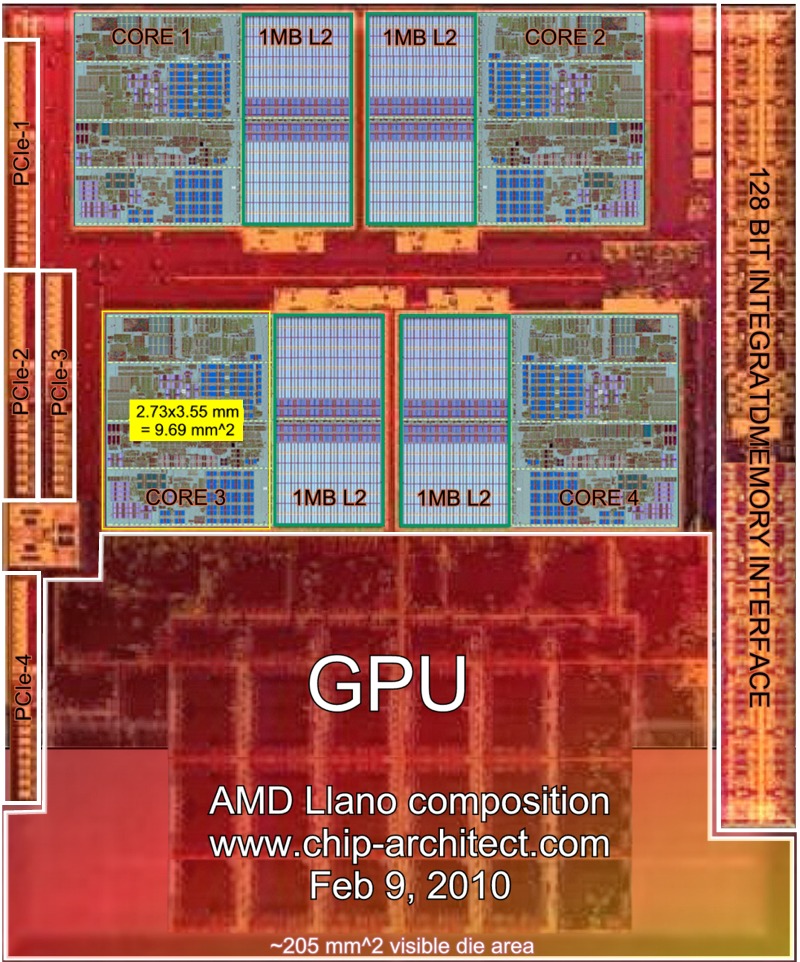
Could you distinguish the HT ports from PCIe Lanes/ports ?Originally Posted by Hans de Vries

AMD earlier said that Fusion parts will come with PCIe Gen 2, only. So there should not be any Hypertransport at all.
There are also no NB chipsets mentioned in the table from above, only a SB part (Hudson).
Thus the ports that you named HT2 & HT3 are probably PCIe connectors that could be used for a dedicated graphic card (2x x8).
Another link will be probably used to connect to the southbridge, ATIs ALink is nothing more then a relabeled PCIe.
The last link could be used for anything else, PCIe x1 Slots, onboard chips, etc.
Furthermore the square die area below HT2 and HT3 and above HT4: Could that be the PCIe logic ?
cheers


 Reply With Quote

Bookmarks