MMM
Page 2 of 4 FirstFirst 1234 LastLast
Results 26 to 50 of 82

Thread: AMD talks up its first Fusion chip

  1. #26
    Xtreme Addict
    Join Date
    Jan 2009
    Posts
    1,445
    gpu does not connect by hypertransport.


    http://www.theregister.co.uk/2010/02..._chip_preview/


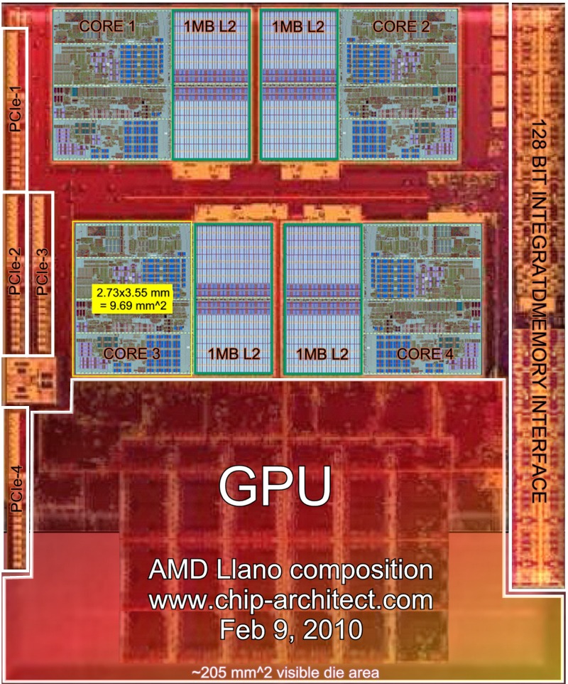
    According to Sam Naffziger, a senior fellow at AMD, the Llano chip will use a 32 nanometer silicon-on insulator process and will have an on-chip DDR3 main memory controller as well as four cores and a DirectX 11 compatible GPU on the die. Naffziger would not divulge the feeds and speeds of the graphics unit, but he said that the GPU is a derivative of the current Radeon HD5000 series and that it will not link to the cores through a HyperTransport link. Instead, it will use a more direct link on the die. The architectural specifics of that link are not being discussed today at ISSCC.
    [MOBO] Asus CrossHair Formula 5 AM3+
    [GPU] ATI 6970 x2 Crossfire 2Gb
    [RAM] G.SKILL Ripjaws X Series 16GB (4 x 4GB) 240-Pin DDR3 1600
    [CPU] AMD FX-8120 @ 4.8 ghz
    [COOLER] XSPC Rasa 750 RS360 WaterCooling
    [OS] Windows 8 x64 Enterprise
    [HDD] OCZ Vertex 3 120GB SSD
    [AUDIO] Logitech S-220 17 Watts 2.1

  2. #27
    Xtreme Addict
    Join Date
    Jan 2007
    Location
    Brisbane, Australia
    Posts
    1,264
    Regor would be the closest thing to compare per/core performance to obviously.

  3. #28
    Xtreme Member
    Join Date
    Sep 2008
    Posts
    235
    Quote Originally Posted by vietthanhpro View Post
    Hypertranport 3.1: 3.2Ghz
    -> HyperTranport 4.0 : 6.4Ghz.
    Hi Vietthanpro,


    I probably should have said 6.4 Gb/s (=HT3.1) anything above that
    is speculation. I could believe higher speeds on a MCM (multi chip module)

    There is a lot going on in the industry to get to higher serial
    communication speeds. For instance some recent news:

    Engineers explore life beyond 10 Gbit links
    Designers rally around 25G, but next step still a mystery
    http://www.eetimes.com/news/design/s...2700195&pgno=1

    Altera to offer partial reconfiguration at 28-nm
    28-Gbps transceivers, embed hard IP also on slate
    http://www.eetimes.com/news/latest/s...leID=222600544

    Regards, Hans

  4. #29
    Xtreme Member
    Join Date
    Sep 2008
    Posts
    235
    Quote Originally Posted by Firestrider View Post
    is dual channel ddr3 going to be enough bandwidth for both the gpu and cpu?
    That's the big mystery question... How do they solve the bandwidth needs.
    I somehow thrust the ATI engineers that they made sure that that's ok.

    Maybe on a part of the die which hasn't been shown in public yet. or
    maybe in cooperation with the DRAM industry + rival NVidia. It's possible
    to put main memory in GDDR5 using TSV (Through Silicon Via's) die stacks.
    Elpida is already supplying DDR3 TSV die stacks with 8 memory chips in a
    package. The 9th chip is the interface chip which can in principle be
    replaced by a GDDR5 interface chip.


    Regards, Hans

  5. #30
    Xtreme Addict
    Join Date
    Dec 2007
    Location
    Hungary (EU)
    Posts
    1,376
    Quote Originally Posted by Hans de Vries View Post
    That's the big mystery question... How do they solve the bandwidth needs.
    I somehow thrust the ATI engineers that they made sure that that's ok.

    Maybe on a part of the die which hasn't been shown in public yet. or
    maybe in cooperation with the DRAM industry + rival NVidia. It's possible
    to put main memory in GDDR5 using TSV (Through Silicon Via's) die stacks.
    Elpida is already supplying DDR3 TSV die stacks with 8 memory chips in a
    package. The 9th chip is the interface chip which can in principle be
    replaced by a GDDR5 interface chip.


    Regards, Hans


    128-bit, 512MB GDDR3 (E4690 MXM)

    Is it possible that those "HT links" are single channel GDDR controllers?
    -

  6. #31
    Xtreme Enthusiast
    Join Date
    Feb 2005
    Posts
    970
    Is the Fusion Memory Controller supposed to be implimented on Llano also, or just Bulldozer derivatives? I'm looking forwared to details on that FMC, but that info probably won't be released for a while.

  7. #32
    Xtreme Member
    Join Date
    Aug 2004
    Posts
    210
    Quote Originally Posted by Hans de Vries View Post
    Later die pictures showed more GPU area so the die for so far is ~205mm^2

    Could you distinguish the HT ports from PCIe Lanes/ports ?
    AMD earlier said that Fusion parts will come with PCIe Gen 2, only. So there should not be any Hypertransport at all.


    There are also no NB chipsets mentioned in the table from above, only a SB part (Hudson).

    Thus the ports that you named HT2 & HT3 are probably PCIe connectors that could be used for a dedicated graphic card (2x x8).
    Another link will be probably used to connect to the southbridge, ATIs ALink is nothing more then a relabeled PCIe.

    The last link could be used for anything else, PCIe x1 Slots, onboard chips, etc.

    Furthermore the square die area below HT2 and HT3 and above HT4: Could that be the PCIe logic ?

    cheers
    Last edited by Opteron146; 02-09-2010 at 08:16 AM.

  8. #33
    Xtreme Member
    Join Date
    Sep 2008
    Posts
    235
    Quote Originally Posted by Opteron146 View Post
    Could you distinguish the HT ports from PCIe Lanes/ports ?
    AMD earlier said that Fusion parts will come with PCIe Gen 2, only. So there should not be any Hypertransport at all.


    There are also no NB chipsets mentioned in the table from above, only a SB part (Hudson).

    Thus the ports that you named HT2 & HT3 are probably PCIe connectors that could be used for a dedicated graphic card (2x x8).
    Another link will be probably used to connect to the southbridge, ATIs ALink is nothing more then a relabeled PCIe.

    The last link could be used for anything else, PCIe x1 Slots, onboard chips, etc.

    Furthermore the square die area below HT2 and HT3 and above HT4: Could that be the PCIe logic ?

    cheers

    You are right Opteron146 according to the presentation.
    The PCIe lanes have moved from the chip-set to the CPU/GPU die.
    The Llano compilation is already updated.


    Regards, Hans

  9. #34
    Banned
    Join Date
    Jun 2008
    Location
    Mi
    Posts
    1,063
    Did anyone see Flipp'n_Waff's response to Kyle...? lol hilarious.

  10. #35
    Xtreme Member
    Join Date
    Jul 2004
    Location
    Berlin
    Posts
    275
    Quote Originally Posted by Hans de Vries View Post
    You are right Opteron146 according to the presentation.
    The PCIe lanes have moved from the chip-set to the CPU/GPU die.
    The Llano compilation is already updated.


    Regards, Hans
    An even higher res Llano shot can be found at
    http://www.pcgameshardware.de/aid,70...fikkarte/News/:

    (Thanks to Opteron@Planet3dnow! for the copy - the same as Opteron146 here?)

    This might be interesting for core comparisons, for example to find out, what this is (APM? more TLBs? or related to dynamic cache resizing?):

    .
    Now on Twitter: @Dresdenboy!
    Blog: http://citavia.blog.de/

  11. #36
    Xtreme Member
    Join Date
    Aug 2004
    Posts
    210
    Quote Originally Posted by Dresdenboy View Post
    (Thanks to Opteron@Planet3dnow! for the copy - the same as Opteron146 here?)
    Klar, wer sonst

  12. #37
    Xtreme Addict
    Join Date
    Jan 2009
    Posts
    1,445
    Quote Originally Posted by Xoulz View Post
    Did anyone see Flipp'n_Waff's response to Kyle...? lol hilarious.

    lol omfg i just saw it lol, here is a link, check out the comments.


    http://blogs.amd.com/fusion/2010/02/...ovation-isscc/
    [MOBO] Asus CrossHair Formula 5 AM3+
    [GPU] ATI 6970 x2 Crossfire 2Gb
    [RAM] G.SKILL Ripjaws X Series 16GB (4 x 4GB) 240-Pin DDR3 1600
    [CPU] AMD FX-8120 @ 4.8 ghz
    [COOLER] XSPC Rasa 750 RS360 WaterCooling
    [OS] Windows 8 x64 Enterprise
    [HDD] OCZ Vertex 3 120GB SSD
    [AUDIO] Logitech S-220 17 Watts 2.1

  13. #38
    Xtreme Cruncher
    Join Date
    Jun 2006
    Posts
    6,215
    Kyle is just being his "natural" self... He just can't help making a fool of himself,even publicly in front of some AMD's VPs.

  14. #39
    Xtreme Member
    Join Date
    Sep 2008
    Posts
    235
    Quote Originally Posted by Dresdenboy View Post
    An even higher res Llano shot can be found at
    http://www.pcgameshardware.de/aid,70...fikkarte/News/:

    (Thanks to Opteron@Planet3dnow! for the copy - the same as Opteron146 here?)

    This might be interesting for core comparisons, for example to find out, what this is (APM? more TLBs? or related to dynamic cache resizing?):

    .
    Nice find! There's one slightly bigger version over there:


    Regards, Hans

  15. #40
    Xtreme Mentor
    Join Date
    Apr 2005
    Posts
    2,550
    Quote Originally Posted by god_43 View Post
    lol omfg i just saw it lol, here is a link, check out the comments.


    http://blogs.amd.com/fusion/2010/02/...ovation-isscc/
    it's funny that moderator closed one eye on Flippin's sincere advice
    Adobe is working on Flash Player support for 64-bit platforms as part of our ongoing commitment to the cross-platform compatibility of Flash Player. We expect to provide native support for 64-bit platforms in an upcoming release of Flash Player following the release of Flash Player 10.1.

  16. #41
    Xtreme Member
    Join Date
    Aug 2004
    Posts
    210
    Quote Originally Posted by Hans de Vries View Post
    Nice find! There's one slightly bigger version over there:

    http://www.pcgameshardware.de/screen...o-Vierkern.jpg
    Haha, same error as over @P3D, there is just a small "No Deeplink" message.
    But it seems that I got a downsized picture last time, or PCGH changed the pic in the meantime.

    Anyways, here's the pic:


    @Dresdenboy:
    I'll change it over at P3D, too.
    One idea for the changed area: Maybe some changes in the cache controller, due to the 8T cache cells (K10 had 6T) ?

    cheers

    Alex
    Last edited by Opteron146; 02-09-2010 at 07:05 PM.

  17. #42
    Xtreme Member
    Join Date
    Aug 2008
    Location
    Australia
    Posts
    373
    Amidst all this technical talk, can someone please explain whether or not the on-die GPU for Llano and other fusion products will benefit the average user who already has a GPU? If so, how? Will the CPU distribute workloads to the GPU? I've heard that GPU is better at calculating/computing certain jobs than CPUs (ie all that GPGPU stuff).

  18. #43
    Xtreme Enthusiast
    Join Date
    Feb 2005
    Posts
    970
    Well geez, I remember having a discussion with Kyle on [H], where his argument was that the Phenom II chip was a pile of crap and that the headroom for O/Cing was worthless because it never added any value to the chip and wouldn't help AMD sell any. It's not what customers wanted. How crazy is that, on an enthusiast website no less! And I especially liked his Eyefinity review where he had boxes and boxes of intel processors piled up in the backround in plain site. I'm sure that added some good advertising dollars. It's pretty clear which brand he prefers at the moment, but come on, still harping on the move from 45nm to 32nm for Bulldozer? How old is that. Anyway, I really didn't expect it would get approved.

    BTW, I was reading the comments on Dresdenboy's blog. Any truth to that one about the much improved front end here?

  19. #44
    Xtreme Member
    Join Date
    Aug 2004
    Posts
    210
    Quote Originally Posted by flippin_waffles View Post
    BTW, I was reading the comments on Dresdenboy's blog. Any truth to that one about the much improved front end here?
    I guess he was referring to the discussion @amdzone:
    http://www.amdzone.com/phpbb3/viewto...0d27&start=500

    No proof, just a patent.

  20. #45
    Xtreme Member
    Join Date
    Jul 2004
    Location
    Berlin
    Posts
    275
    Quote Originally Posted by Opteron146 View Post
    @Dresdenboy:
    I'll change it over at P3D, too.
    One idea for the changed area: Maybe some changes in the cache controller, due to the 8T cache cells (K10 had 6T) ?
    BTW, yesterday I looked for any reference to 8T cache cells in the reports and didn't find anything or overlooked it. IIRC, this subtopic has been announced for this ISSCC.
    Now on Twitter: @Dresdenboy!
    Blog: http://citavia.blog.de/

  21. #46
    Xtreme Member
    Join Date
    Aug 2004
    Posts
    210
    Quote Originally Posted by Dresdenboy View Post
    BTW, yesterday I looked for any reference to 8T cache cells in the reports and didn't find anything or overlooked it. IIRC, this subtopic has been announced for this ISSCC.
    Yes, it was mentioned earlier in an eetimes article:
    Much of AMD's paper will focus on circuit techniques the company is using to lower power consumption and leakage of the core. For example, the core's L1 cache uses 8T memory cells to support low supply voltages.
    http://www.eetimes.com/rss/showArtic...leID=221900830

    I guess they just forgot that in the telephone conference. IMO, there are still no real ISSCC articles.

  22. #47
    Xtreme Addict
    Join Date
    Apr 2006
    Posts
    2,462
    Quote Originally Posted by Opteron146 View Post
    @Dresdenboy:
    I'll change it over at P3D, too.
    One idea for the changed area: Maybe some changes in the cache controller, due to the 8T cache cells (K10 had 6T) ?

    cheers

    Alex
    Does 6T mean six transistors per cache cell? So Llano's cache might need more space for the same amount, but on the other hand need less energy?

    P.S. Dann bist du wohl auch der Opteron der im Luxx sein "Unwesen" treibt, was? :P
    Notice any grammar or spelling mistakes? Feel free to correct me! Thanks

  23. #48
    Xtreme Member
    Join Date
    Sep 2008
    Posts
    235
    Quote Originally Posted by Oliverda View Post


    128-bit, 512MB GDDR3 (E4690 MXM)

    Is it possible that those "HT links" are single channel GDDR controllers?
    I would like to see Graphics GDDR5 memory in the package yes :^)
    If they still hide some of the lower part of the die, then this may be
    the reason. The extra memory interface would be very easy to spot.

    The other solution, the better one in the long term, is to raise the
    128 bit IMC to GDDR5 speeds. This would currently limit the main
    memory size. Fermi will use up to 2GB per 128bit databus in the 2nd
    half of this year. However, this could rapidly increase with the use
    of TSV stacked dies. I guess 4GB to 8GB of GDDR5 main memory
    would be enough for 2011.


    Regards, Hans

  24. #49
    Xtreme Member
    Join Date
    Sep 2008
    Posts
    235
    Quote Originally Posted by FischOderAal View Post
    Does 6T mean six transistors per cache cell? So Llano's cache might need more space for the same amount, but on the other hand need less energy?
    The blocks containing the L1 data and instruction cache are some 10%
    wider relatively compared to the 45nm layout because of the larger 8T
    cells. Intel uses 8T cells for the L1 caches at 32nm at well.

    The extra room is used for the extra logic Mathias was talking about.


    Regards, Hans

  25. #50
    Xtreme Member
    Join Date
    Jul 2004
    Location
    Berlin
    Posts
    275
    Charlie Demerjian has his Llano article up with a lot of new details:
    http://www.semiaccurate.com/2010/02/...nm-llano-core/

    My thoughts are here:
    http://citavia.blog.de/2010/02/11/mo...tails-7987376/

    There is still room for surprises..
    Now on Twitter: @Dresdenboy!
    Blog: http://citavia.blog.de/

Page 2 of 4 FirstFirst 1234 LastLast

Bookmarks

Bookmarks

Posting Permissions

  • You may not post new threads
  • You may not post replies
  • You may not post attachments
  • You may not edit your posts
  •