MMM
Results 1 to 25 of 82

Thread: AMD talks up its first Fusion chip

Hybrid View

  1. #1
    Xtreme Addict
    Join Date
    Apr 2008
    Location
    Lansing, MI / London / Stinkaypore
    Posts
    1,788


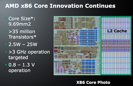
    Core = 9.69mm^2
    Core + L2 ~ 1.5x of that? = ~15mm^2

    So basically quadcore logic under 90mm^2 (+IMC,HTPad...)?


    IMO the total die size should be 140-180mm^2 or so, but no longer do they have to sell it at $99- fetching double the price should be easy, not that it would be a good purchase for desktop.

    For laptops though I think this should be their way in, especially with the emphasis on power management- seems to me that this is a laptop oriented design for the most part, being able to target $300+ ASPs that AMD could previously only dream about.
    Last edited by Macadamia; 02-08-2010 at 02:59 PM.
    Quote Originally Posted by radaja View Post
    so are they launching BD soon or a comic book?

  2. #2
    Xtreme Member
    Join Date
    Sep 2008
    Posts
    235
    Quote Originally Posted by Macadamia View Post
    Core = 9.69mm^2
    Core + L2 ~ 1.5x of that? = ~15mm^2

    So basically quadcore logic under 90mm^2 (+IMC,HTPad...)?


    IMO the total die size should be 140-180mm^2 or so, but no longer do they have to sell it at $99- fetching double the price should be easy, not that it would be a good purchase for desktop.

    For laptops though I think this should be their way in, especially with the emphasis on power management- seems to me that this is a laptop oriented design for the most part, being able to target $300+ ASPs that AMD could previously only dream about.
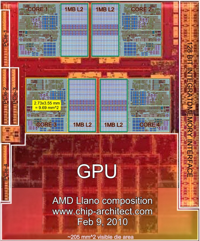
    Later die pictures showed more GPU area so the die for so far is ~205mm^2


    Regards, Hans

  3. #3
    Xtreme Enthusiast
    Join Date
    Oct 2007
    Location
    Hong Kong
    Posts
    526
    Quote Originally Posted by Hans de Vries View Post
    Later die pictures showed more GPU area so the die for so far is ~205mm^2


    Regards, Hans
    why there are 4 hypertransport links?

  4. #4
    Xtreme Addict
    Join Date
    Jun 2002
    Location
    Ontario, Canada
    Posts
    1,782
    Quote Originally Posted by qcmadness View Post
    why there are 4 hypertransport links?
    Just a guess...Hans will obviously know more.

    1 HT link to the GPU.
    1 or 2 HT link(s) between the CPU cores.
    1 HT link to the rest of the system. (PCI-E bus, southbridge, add in card, etc...)
    Last edited by freeloader; 02-08-2010 at 07:25 PM.
    As quoted by LowRun......"So, we are one week past AMD's worst case scenario for BD's availability but they don't feel like communicating about the delay, I suppose AMD must be removed from the reliable sources list for AMD's products launch dates"

  5. #5
    Xtreme Member
    Join Date
    Sep 2008
    Posts
    235
    Quote Originally Posted by freeloader View Post
    Just a guess...Hans will obviously know more.

    1 HT link to the GPU.
    1 or 2 HT link(s) between the CPU cores.
    1 HT link to the rest of the system. (PCI-E bus, southbridge, add in card, etc...)

    Yes, interesting all these HT links... They are half width but probably
    almost as fast as the full width HT's used up to now (>=6.4GHz)

    Maybe for 2 dies per package for higher performance desktops?

    or also for the HPC market (CRAY) to build supercomputers getting
    a whole lot more TFlops from the GPU's?

    or maybe one is used to transport monitor output data to the
    South bridge?

    Regards, Hans
    Last edited by Hans de Vries; 02-08-2010 at 08:10 PM.

  6. #6
    Xtreme Member
    Join Date
    Nov 2008
    Posts
    117
    Quote Originally Posted by Hans de Vries View Post
    Yes, interesting all these HT links... They are half width but probably
    almost as fast as the full width HT's used up to now (>=6.4GHz)

    Maybe for 2 dies per package for higher performance desktops?

    or also for the HPC market (CRAY) to build supercomputers getting
    a whole lot more TFlops from the GPU's?

    or maybe one is used to transport monitor output data to the
    South bridge?

    Regards, Hans
    Hypertranport 3.1: 3.2Ghz
    -> HyperTranport 4.0 : 6.4Ghz.
    When AMD had 64-bit and Intel had only 32-bit, they tried to tell the world there was no need for 64-bit. Until they got 64-bit.
    When AMD had IMC and Intel had FSB, they told the world "there is plenty of life left in the FSB" (actual quote, and yes, they had *math* to show it had more bandwidth). Until they got an IMC.
    When AMD had dual core and Intel had single core, they told the world that consumers don't need multi core. Until they got dual core.
    When intel was using MCM, they said it was a better solution than native dies. Until they got native dies. (To be fair, we knocked *unconnected* MCM, and still do, we never knocked MCM as a technology, so hold your flames.)
    by John Fruehe

  7. #7
    Xtreme Member
    Join Date
    Sep 2008
    Posts
    235
    Quote Originally Posted by vietthanhpro View Post
    Hypertranport 3.1: 3.2Ghz
    -> HyperTranport 4.0 : 6.4Ghz.
    Hi Vietthanpro,


    I probably should have said 6.4 Gb/s (=HT3.1) anything above that
    is speculation. I could believe higher speeds on a MCM (multi chip module)

    There is a lot going on in the industry to get to higher serial
    communication speeds. For instance some recent news:

    Engineers explore life beyond 10 Gbit links
    Designers rally around 25G, but next step still a mystery
    http://www.eetimes.com/news/design/s...2700195&pgno=1

    Altera to offer partial reconfiguration at 28-nm
    28-Gbps transceivers, embed hard IP also on slate
    http://www.eetimes.com/news/latest/s...leID=222600544

    Regards, Hans

  8. #8
    Xtreme X.I.P.
    Join Date
    Nov 2002
    Location
    Shipai
    Posts
    31,147
    cheers

    Quote Originally Posted by Hans de Vries View Post
    Yes, interesting all these HT links... They are half width but probably
    almost as fast as the full width HT's used up to now (>=6.4GHz)

    Maybe for 2 dies per package for higher performance desktops?

    or also for the HPC market (CRAY) to build supercomputers getting
    a whole lot more TFlops from the GPU's?

    or maybe one is used to transport monitor output data to the
    South bridge?

    Regards, Hans
    hmmmm the latter makes a lot of sense... but do they need a seperate HT link for that? thats what confused me about intel as well, why dont they use that massive qpi bus to move all the display data

  9. #9
    Xtreme Addict
    Join Date
    May 2007
    Location
    'Zona
    Posts
    2,346
    Have we seen stacked HT links before???
    Originally Posted by motown_steve
    Every genocide that was committed during the 20th century has been preceded by the disarmament of the target population. Once the government outlaws your guns your life becomes a luxury afforded to you by the state. You become a tool to benefit the state. Should you cease to benefit the state or even worse become an annoyance or even a hindrance to the state then your life becomes more trouble than it is worth.

    Once the government outlaws your guns your life is forfeit. You're already dead, it's just a question of when they are going to get around to you.

  10. #10
    Xtreme Member
    Join Date
    Aug 2004
    Posts
    210
    Quote Originally Posted by Hans de Vries View Post
    Later die pictures showed more GPU area so the die for so far is ~205mm^2

    Could you distinguish the HT ports from PCIe Lanes/ports ?
    AMD earlier said that Fusion parts will come with PCIe Gen 2, only. So there should not be any Hypertransport at all.


    There are also no NB chipsets mentioned in the table from above, only a SB part (Hudson).

    Thus the ports that you named HT2 & HT3 are probably PCIe connectors that could be used for a dedicated graphic card (2x x8).
    Another link will be probably used to connect to the southbridge, ATIs ALink is nothing more then a relabeled PCIe.

    The last link could be used for anything else, PCIe x1 Slots, onboard chips, etc.

    Furthermore the square die area below HT2 and HT3 and above HT4: Could that be the PCIe logic ?

    cheers
    Last edited by Opteron146; 02-09-2010 at 08:16 AM.

  11. #11
    Xtreme Member
    Join Date
    Sep 2008
    Posts
    235
    Quote Originally Posted by Opteron146 View Post
    Could you distinguish the HT ports from PCIe Lanes/ports ?
    AMD earlier said that Fusion parts will come with PCIe Gen 2, only. So there should not be any Hypertransport at all.


    There are also no NB chipsets mentioned in the table from above, only a SB part (Hudson).

    Thus the ports that you named HT2 & HT3 are probably PCIe connectors that could be used for a dedicated graphic card (2x x8).
    Another link will be probably used to connect to the southbridge, ATIs ALink is nothing more then a relabeled PCIe.

    The last link could be used for anything else, PCIe x1 Slots, onboard chips, etc.

    Furthermore the square die area below HT2 and HT3 and above HT4: Could that be the PCIe logic ?

    cheers

    You are right Opteron146 according to the presentation.
    The PCIe lanes have moved from the chip-set to the CPU/GPU die.
    The Llano compilation is already updated.


    Regards, Hans

  12. #12
    Xtreme Member
    Join Date
    Jul 2004
    Location
    Berlin
    Posts
    275
    Quote Originally Posted by Hans de Vries View Post
    You are right Opteron146 according to the presentation.
    The PCIe lanes have moved from the chip-set to the CPU/GPU die.
    The Llano compilation is already updated.


    Regards, Hans
    An even higher res Llano shot can be found at
    http://www.pcgameshardware.de/aid,70...fikkarte/News/:

    (Thanks to Opteron@Planet3dnow! for the copy - the same as Opteron146 here?)

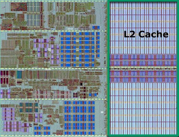
    This might be interesting for core comparisons, for example to find out, what this is (APM? more TLBs? or related to dynamic cache resizing?):

    .
    Now on Twitter: @Dresdenboy!
    Blog: http://citavia.blog.de/

  13. #13
    Xtreme Member
    Join Date
    Aug 2004
    Posts
    210
    Quote Originally Posted by Dresdenboy View Post
    (Thanks to Opteron@Planet3dnow! for the copy - the same as Opteron146 here?)
    Klar, wer sonst

  14. #14
    Xtreme Member
    Join Date
    Sep 2008
    Posts
    235
    Quote Originally Posted by Dresdenboy View Post
    An even higher res Llano shot can be found at
    http://www.pcgameshardware.de/aid,70...fikkarte/News/:

    (Thanks to Opteron@Planet3dnow! for the copy - the same as Opteron146 here?)

    This might be interesting for core comparisons, for example to find out, what this is (APM? more TLBs? or related to dynamic cache resizing?):

    .
    Nice find! There's one slightly bigger version over there:


    Regards, Hans

  15. #15
    Xtreme Member
    Join Date
    Aug 2004
    Posts
    210
    Quote Originally Posted by Hans de Vries View Post
    Nice find! There's one slightly bigger version over there:

    http://www.pcgameshardware.de/screen...o-Vierkern.jpg
    Haha, same error as over @P3D, there is just a small "No Deeplink" message.
    But it seems that I got a downsized picture last time, or PCGH changed the pic in the meantime.

    Anyways, here's the pic:


    @Dresdenboy:
    I'll change it over at P3D, too.
    One idea for the changed area: Maybe some changes in the cache controller, due to the 8T cache cells (K10 had 6T) ?

    cheers

    Alex
    Last edited by Opteron146; 02-09-2010 at 07:05 PM.

  16. #16
    Registered User
    Join Date
    Feb 2010
    Location
    Poland
    Posts
    6
    Quote Originally Posted by Dresdenboy View Post
    An even higher res Llano shot can be found at
    This might be interesting for core comparisons, for example to find out, what this is (APM? more TLBs? or related to dynamic cache resizing?):

    .
    I see more changes:

    Longer Shedulers or ALU/AGUs ??
    Increased reorder buffer ??
    New unit next to the FPU register?? (currently it is empty space)


  17. #17
    Xtreme Member
    Join Date
    Aug 2004
    Posts
    210
    Quote Originally Posted by Zibi View Post
    I see more changes:

    Longer Shedulers or ALU/AGUs ??
    Increased reorder buffer ??
    Yes, this is mentioned in the articles linked previously:
    http://www.xtremesystems.org/forums/...2&postcount=50
    New unit next to the FPU register?? (currently it is empty space)
    I think that's new ;-)
    I assume that it has something to do with SSSE3/SSSE4.1. When AMD doubled the FPU from 64->128bit they basically copied the whole 64bit FPU. However there was some empty space in the end which was used for old 3DNOW! stuff and need not to be doubled. Thus it would be logical, if AMD uses that free space in the doubled FPU part with another instruction set extension.

    Welcome to XS

    Opteron146

  18. #18
    Xtreme Member
    Join Date
    Jul 2004
    Location
    Berlin
    Posts
    275
    Quote Originally Posted by Zibi View Post
    I see more changes:

    Longer Shedulers or ALU/AGUs ??
    Increased reorder buffer ??
    New unit next to the FPU register?? (currently it is empty space)
    Additional to what Opteron146 pointed out, there was another update over 2 months ago:
    http://citavia.blog.de/2010/02/09/so...o-die-7974978/

    There is also something new in the L/S unit plus new D$ tags.
    The ALU/AGU block became longer at the int multiplier end, maybe related to a lower power multiplier implementation or the already mentioned hardware divider support.
    Now on Twitter: @Dresdenboy!
    Blog: http://citavia.blog.de/

Bookmarks

Bookmarks

Posting Permissions

  • You may not post new threads
  • You may not post replies
  • You may not post attachments
  • You may not edit your posts
  •