 Home / Play Rig
 Asrock Z87 OC Formula/AC, i7 4770K L310B487, 8GB Corsair Dominator Platinum 2666 CL10, BeQuiet Dark Power Pro P8 1200W PSU, 120GB Corsair Force GT SSD, 2 x 1TB WD Sata Drives Mirrored, Palit 680GTX JetStream, Antec Kuhler 920, Windows 10 Pro, Logitech LX700 Deskset, AOC 27" Monitor.
Work 24/7 Rig Gigabyte GA-Z97X-SOC Force, i7 4790K L418C133 ,8GB Team Xtreem LV 2600, PC Power & Cooling 850WPSU, 120GB OCZ Vertex 3 SSD, 2 x 500GB Hitachi Sata Drives Mirrored, Antec Kuhler 620, Windows 10 Pro 64 Bit, Logitech LX700 Deskset, Benq 27" Monitor.
Home NAS DFI P35 T2RL Motherboard, Intel E6850 CPU, 8GB Nanya DDR2 6400, 2X 2TB Toshiba DT01ACA200 SATA Drives, ZFS RAID Mirror On Intel ICH9 AHCI, Artic Blue 850W PSU, Marvell Yukon 88E8053 Gigabit Ethernet, FreeNAS 9.2.1.5 RC, 64-Bit On 4GB USB2 SanDisk Cruizer Blade Thumb Drive.


did they fix this yet with a bios update...if any has an answer i would appreciate it...thanks
 i7 920 4.2ghz..6gb 1600mhz cas 7 memory..Windows 7 Ultimate Edition..Windows XP..650 watt PS..Water..3DFX Voodoo 3
 Reply With Quote


 I'll post up my settings if it runs a loop properly.
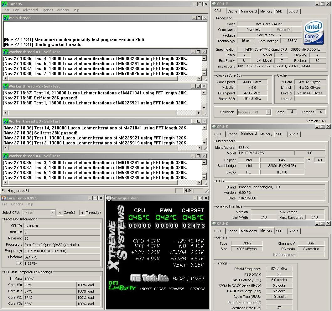


 so here's the settings I used.
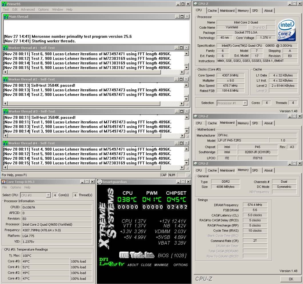


 1240mhz@2.02v


Bookmarks