


Tested this last night it passed linpack 10 loop testOriginally Posted by electricl

Extreme Tweaker
Ai Overclock Tuner : Manual
OC From CPU Level Up : AUTO
CPU Ratio Control : Manual
- Ratio CMOS Setting : 8
FSB Frequency : 500
CPU Clock Skew : Normal
North Bridge Clock Skew : Normal
FSB Strap to North Bridge : Auto
DRAM Frequency: DDR2-1000
Dram Clock Skew CH1 A1 : Auto
DRAM Clock Skew CH1 A2 : Auto
Dram Clock Skew CH1 B1 : Auto
Dram Clock Skew CH1 B2 : Auto
DRAM Timing Control: Manual
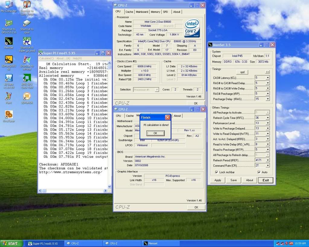
CAS# Latency : 5
RAS# to CAS# Delay : 5
RAS# Precharge : 5
RAS# ActivateTime : 15
RAS# to RAS# Delay : 3
Row Refresh Cycle Time : 55
Write Recovery Time : 6
Read to Precharge Time : 3
Read to Write Delay (S/D) : 8
Write to Read Delay (S) : 3
Write to Read Delay (D) : 5
Read to Read Delay (S) : 4
Read to Read Delay (D) : 6
Write to Write Delay (S) : 4
Write to Write Delay (D) : 6
Write to PRE Delay : 14
Read to PRE Delay : 5
PRE to PRE Delay : 1
ALL PRE to ACT Delay : 5
ALL PRE to REF Delay : 5
DRAM Static Read Control: Enabled
Dram Read Training : AUTO
MEM OC Charger : Enabled
Ai Clock Twister : Stronger
Transaction Booster : Manual
Common Performance Level [8]
Pull-In of CHA PH1 Disabled
Pull-In of CHA PH2 Disabled
Pull-In of CHA PH3 Disabled
Pull-In of CHA PH4 Disabled
Pull-In of CHA PH5 Disabled
Pull-In of CHB PH1 Disabled
Pull-In of CHB PH2 Disabled
Pull-In of CHB PH3 Disabled
Pull-In of CHB PH4 Disabled
Pull-In of CHB PH5 Disabled
PCIE Frequency : 100
CPU Voltage : Whatever you think maybe 1.375 to start.
CPU PLL Voltage : 1.55
FSBT : 1.33850
DRAM Voltage : 2.12
North Bridge Voltage : 1.39150
South Bridge Voltage 1.5 : 1.5
South Bridge Voltage 1.1 : 1.1
CPU GTL Reference 0 : +20mv
CPU GTL Reference 1 : +20mv
CPU GTL Reference 2 : +20mv
CPU GTL Reference 3 : +20mv
North Bridge GTL Reference : AUTO
DDR2 Channel A REF Voltage : AUTO
DDR2 Channel B REF Voltage : AUTO
North Bridge DDR Reference : AUTO
Load Line Calabration : Enabled
CPU Sread Spectrum : Disabled
PCIE Spread Spectrum : Disabled


 Reply With Quote


 does the board have pretty LED lights too? if it does I might not be able to resist....
 i really dont want to rma it


Bookmarks