

Same site, same topic, different result:Originally Posted by savantu

http://www.semiconductor.net/article...Generation.php
Seems, we have to wait and watch how the story unfolds.


Same site, same topic, different result:
http://www.semiconductor.net/article...Generation.php
Seems, we have to wait and watch how the story unfolds.
@dresdenboy. this is from your blog.
perhaps endian byte order?Does someone have an idea, what EBO is?
Ah, OK. This riddle is already solved.Please have a look at the comments to my blog entry.
Hey, someone has to assume the role of the optimist!
Hopefully AMD is not going down the same road as Intel tried to with the P4 Netburst path or if they are, hopefully they've
learned enough to not make the mistakes Intel did. I had a Prescott that I could literally heat up my computer room with.
Last edited by freeloader; 01-27-2010 at 01:22 PM.
IMC design is not good for battery performance
while you shut down cpu, you cannot power down imc because (i)gpu needs it
something about this design makes me believe that ipc is going to be really high? intel has 4 per cycle right? or do i have this mixed up with something else?
[MOBO] Asus CrossHair Formula 5 AM3+
[GPU] ATI 6970 x2 Crossfire 2Gb
[RAM] G.SKILL Ripjaws X Series 16GB (4 x 4GB) 240-Pin DDR3 1600
[CPU] AMD FX-8120 @ 4.8 ghz
[COOLER] XSPC Rasa 750 RS360 WaterCooling
[OS] Windows 8 x64 Enterprise
[HDD] OCZ Vertex 3 120GB SSD
[AUDIO] Logitech S-220 17 Watts 2.1
the max. ipc per module (dual-core):
INT: 4
64-bit FP: 4
128-bit FP: 2
256-bit FP: 1
Total issue: 4
if the ALU and FPU are clocked as the same
Last edited by qcmadness; 01-27-2010 at 11:24 PM.
oh.......that is certainly interesting? is this on par with what intel has now then?
[MOBO] Asus CrossHair Formula 5 AM3+
[GPU] ATI 6970 x2 Crossfire 2Gb
[RAM] G.SKILL Ripjaws X Series 16GB (4 x 4GB) 240-Pin DDR3 1600
[CPU] AMD FX-8120 @ 4.8 ghz
[COOLER] XSPC Rasa 750 RS360 WaterCooling
[OS] Windows 8 x64 Enterprise
[HDD] OCZ Vertex 3 120GB SSD
[AUDIO] Logitech S-220 17 Watts 2.1
Not much info for Sandy Bridge except 256-bit AVX extensions (SSEx is 128-bit)
Nehalem / Westmere:
IPC:
INT: 3 (+2)
FP / SSE: 3
Total issue: 4
Last edited by qcmadness; 01-27-2010 at 11:25 PM.
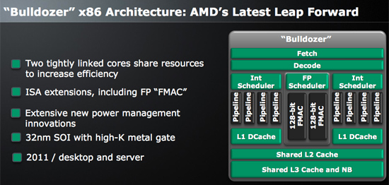
According to AMD's Rick Bergam,each core inside the module is 4 issue wide,so at the module level INT capability is 2x of that,while FP is also 4 issue with 256bit AVX and FMAC capability(FMAC practically stomps anything we have today in x86 world as far as fp/sse stuff goes).
http://www.anandtech.com/cpuchipsets...oc.aspx?i=3674
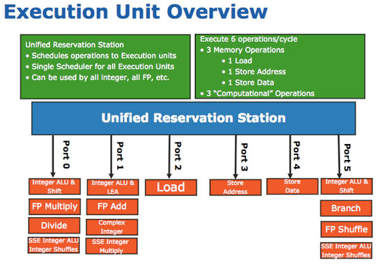
Currently each K10 integer pipeline can do both ALU and memory ops.Within each integer “core” are four pipelines, presumably half for ALUs and half for memory ops. That’s a narrower width than a single Phenom II core, but there are two integer clusters on a single Bulldozer core.

Last edited by qcmadness; 01-28-2010 at 12:49 AM.
Note the key word in AT's speculative article:
In other words he presumes. You have a diagram from AMD stating 4 pipelines(non segmented into ALUs and AGUs). I'm not saying it's 4 issue being made of grouped 4 ALUs/AGUs ,it may be 2 issue with throughput of 4 issue(look at dresdenboy's blog),but I'm still sticking to the image and the post analyst call interview with Rick Bergam who stated that each core inside the module is a 4 issue core.Within each integer “core” are four pipelines, presumably half for ALUs and half for memory ops.
PS Note that in the diagram of 10h you posted,the ALUs and AGUs are grouped together,in pairs... 3 issue made up of 3 groups of ALUs and AGUs. Very same methodology may apply to BD cores.
Last edited by informal; 01-28-2010 at 01:15 AM.
speculations here
if each core in the module has 4 independent ALU and AGUs, the core will be "swelled" and may get too big.
my image for 2 ALU arguments comes from
1. post above (average integer IPC is about 2)
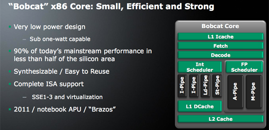
2. bobcat diagram (very similar to half of a bulldozer module)
if the architecture is for server space, then it sounds possible to have only 2 ALU per core as each thread for server application is of low IPC but highly-threaded (>24 thread).
BD and bobcat were developed by 2 different teams with 2 different goals in mind... While they do share some common ideas,Bobcat is targeted at very low power and good mainstream performance ,while BD is targeted for very high performance with advanced power gating technologies in place to control the power draw in various scenarios. Note also that Bobcat has no support for various ISA extensions BD will support and has a much weaker fp unit with no FMAC capability(which is normal for low power design).
As for the "swelled" comment,you seem to forget that BD is going to be produced @ 32nm node,so no,the cores won't be that big in any case. The module itself is probably even going to be smaller than one SB core(with SMT),courtesy of the way AMD designed the very BD module ...
Last edited by informal; 01-28-2010 at 01:53 AM.
even with 32nm, the BD core is not small though.
Shanghai / Deneb single core: ~19mm^2 / 55M transistor
Calculated BD module: ~29mm^2 / 165M transistor (assuming 50% die shrink, ~150% die size claimed from AT's communication with AMD)
Packing 4 modules with 8MB L3 cache, you still get about 180mm^2 die size.
Last edited by qcmadness; 01-28-2010 at 02:06 AM.
i think the two arrow on the diagram are very clear.
AMD is doing big brute force ultra wide pipelines for BD cores.
don't rely to a SINGLE source only
Main Rig:
Processor & Motherboard:AMD Ryzen5 1400 ' Gigabyte B450M-DS3H
Random Access Memory Module:Adata XPG DDR4 3000 MHz 2x8GB
Graphic Card:XFX RX 580 4GB
Power Supply Unit:FSP AURUM 92+ Series PT-650M
Storage Unit:Crucial MX 500 240GB SATA III SSD
Processor Heatsink Fan:AMD Wraith Spire RGB
Chasis:Thermaltake Level 10GTS Black
1 BD module = 2 Deneb cores.
So, 165 M vs 110 M for 2 deneb cores, 29mm vs 38mm. Performance should be higher as well, so i think they are doing a good job.
How exactly is it early when AMD slides themselves point out it is a 2011 product. Not only that but assuming perfect execution by AMD ( which I really doubt ), everything is at the mercy of GF. Which btw, has some issues with process technology.
Savantu, does intel pay your bills? Does it make breakfast for you? Because from how you post, it looks that way.
Somehow, you want AMD to fail, you want them to be late with this product. Nothing from what we know about bulldozer can make us think they will be late, they seem to move fast into the right direction.
AMD is targeting BD class cores for desktop and server for Q2 next year.Think Thuban time frame + 1 year away(Thuban is May this year).
the AMD today is not the AMD you knew yesterday
lolz
Main Rig:
Processor & Motherboard:AMD Ryzen5 1400 ' Gigabyte B450M-DS3H
Random Access Memory Module:Adata XPG DDR4 3000 MHz 2x8GB
Graphic Card:XFX RX 580 4GB
Power Supply Unit:FSP AURUM 92+ Series PT-650M
Storage Unit:Crucial MX 500 240GB SATA III SSD
Processor Heatsink Fan:AMD Wraith Spire RGB
Chasis:Thermaltake Level 10GTS Black
BD cores get sported by HWinfo app.
Gen. 15h,code name Bulldozer. Since BD samples are in AMD's hands,it's logical they get support from some HW identification app. out there.
http://www.hwinfo.com/
Intel Nehalem family: Core i7 (Bloomfield), Xeon 55xx (Nehalem-EP/Gainestown), Xeon W35xx (Nehalem-WS), Nehalem-EX (Beckton), Core i5/i7 (Lynnfield), Core i7 (Clarksfield), Havendale, Auburndale, Xeon (Jasper Forest)
Intel Westmere family: Core i3/i5 Clarkdale, Core i5/i7 Arrandale (+ECC), Westmere-EP, Westmere-WS, Gulftown, Westmere-EX (Eagleton)
Intel EP80579 (Tolapai), Atom Z5xx (Silverthorne), Atom N2xx/2xx/3xx (Diamondville), Atom N4xx/D4xx/D5xx (Pineview), Atom (Lincroft)
Intel Sandy Bridge family
AMD Family 10h (DR-Ax/Bx, RB-Cx, BL-Cx, DA-Cx, HY-Dx, PH-Ex):
- AM2r2/AM3: Athlon/Sempron (Lima, Sargas), Athlon II/Neo (Kuma, Regor, Rana, Propus), Phenom II/Neo (Agena, Deneb, Callisto, Heka, Toliman), TWKR Black Edition
- Fr2/Fr4: Opteron (Barcelona, Shanghai, Suzuka, Budapest, Istanbul)
- G34: Opteron 61xx (Magny Cours)
- S1g3/g4: Turion II/Ultra, Athlon II, Phenom II
- ASB2: Athlon II Neo K, Turion II Neo K
AMD Family 11h (LG-Ax/Bx): S1g2: Sempron SI/NI/X2, Athlon QI/QL (Sable), Turion X2 Ultra/RM (Griffin)
AMD Family 12h (FS1)
AMD Family 15h: Bulldozer
VIA C7 and Nano
intel must know about bulldozers supposed capabilities already eh? i mean intel must have like spy's inside amd (corporate espionage is a big deal you know) im sure? should amd have released any info about these new cpus? is sandyB a new arch, or is it a refresh of nehielem? wont intel be able to counter amd with this info? and why is it snowing out side?
sometimes i think about these things...
[MOBO] Asus CrossHair Formula 5 AM3+
[GPU] ATI 6970 x2 Crossfire 2Gb
[RAM] G.SKILL Ripjaws X Series 16GB (4 x 4GB) 240-Pin DDR3 1600
[CPU] AMD FX-8120 @ 4.8 ghz
[COOLER] XSPC Rasa 750 RS360 WaterCooling
[OS] Windows 8 x64 Enterprise
[HDD] OCZ Vertex 3 120GB SSD
[AUDIO] Logitech S-220 17 Watts 2.1
Amm Intel did delay Sandy bridge and they did it to try and implement something which SB does not have and BD does. Tough the implementation is very hard to accomplish i have been told 3-4 teams are working on it right now, one may call it the v1.1 the v1.0 of SB is all ready for the fight....
If the v1.1 works out it will get relesed in stead of the v1.0 otherwise v1.0 will be used, in tis case IB will come sooner than later.
Coming Soon
 Posting Permissions


 Reply With Quote

Bookmarks