

I'm liking mine more
nVidia-GeForce-GTX-680-Specifications.gif


I'm liking mine more
nVidia-GeForce-GTX-680-Specifications.gif
Originally Posted by Hans de Vries

thats how accurate this entire thread has been
i know this is extremely childish and immature but i simply cant resist saying this. Thats what she said!!
im sorry, i will not revert back to my normal age
GTX680 = GK104
3*32SPs/SM
8 TMUs/SM
4 SMs/GPC
4 GPCs
32 ROPs
256bit bus
2GB 5.0Gbps GDDR5
950MHz core
2*6pin
________
http://forum.beyond3d.com/showpost.p...postcount=1538
Someone found the originals from that OBR fake. Basically background image of a GTX550 and the benchmark slide from a GTX580.
http://forum.beyond3d.com/showpost.p...postcount=1546
I thought that was the point of the joke lol
If that is true, I'm disappointed it isn't coming with a displayport connection.
The majority of their marketshare doesn't care about $500 cards. AMD hasn't effected the sweet spot price on any current gen card. They released a nice enthusiast card for multi-monitor users but this isn't like last gen. Nvidia is competing just fine with ever card in there lineup but GTX580.

So NVIDIA is going to name the mid range GTX 680, fail naming scheme, reminds me when they used the 9800 GTX name as a mid range card.
AMD Threadripper 12 core 1920x CPU OC at 4Ghz | ASUS ROG Zenith Extreme X399 motherboard | 32GB G.Skill Trident RGB 3200Mhz DDR4 RAM | Gigabyte 11GB GTX 1080 Ti Aorus Xtreme GPU | SilverStone Strider Platinum 1000W Power Supply | Crucial 1050GB MX300 SSD | 4TB Western Digital HDD | 60" Samsung JU7000 4K UHD TV at 3840x2160
you should read the post 555 here.if you want i can make it GTX660 or any name if you like. (Thanks to ManofAtlantis on beyond3d)
and the slide for the chart is exactly one used when 580 have been released ... I had suspect something yesterday and so i have just find this one in few sec on Bing images search ( type GTX580 slides ).
I add the white square, less disturbing.
(just have to redo the slide with same color sheme and update the game with new ( Dirt2>Dirt3, BC2 > BF3 etc ), or just mod it.
1 alone it was ok, but not both at same time.. ( its still possible Nvidia will use the old chart and moddifiying it, but it is really doubtfull, the 550 backround image slide you can easy find on the web, he's used for the spec )
Note: OB .... have remove his article and someone have too get this screen and discussed it before http://translate.google.com/translat...icherer-quelle
Last edited by Lanek; 02-09-2012 at 12:11 AM.
CPU: - I7 4930K (EK Supremacy )
GPU: - 2x AMD HD7970 flashed GHZ bios ( EK Acetal Nickel Waterblock H2o)
Motherboard: Asus x79 Deluxe
RAM: G-skill Ares C9 2133mhz 16GB
Main Storage: Samsung 840EVO 500GB / 2x Crucial RealSSD C300 Raid0
nVidia has no incentive at all to lower prices just to hurt AMD. That buys them nothing. If GK104 prices are low it simply means there's another chip coming to occupy the $350-$700 range.
nVidia GK104
Product name (top solution): GeForce GTX 680 (but not entirely sure)
28nm production at TSMC, the area approximately 340mm ² (unofficial estimate)
4 Graphics Processing Cluster (GPC)
4 Streaming Multiprocessors (SM) aka shader clusters per GPC, ergo a total of 16 shader clusters for the GK104-chip
96 stream processors (SP) aka shader shader units per cluster, ergo a total of 1536 shader units for the GK104-chip
8 texture units (TMU) aka shader texture units per cluster, ergo a total of 128 units of textures for the GK104-chip
32 raster operation units (ROPs)
256-bit DDR memory interface (up to GDDR5)
Chip clock (top model): 950 MHz
Elimination of Hotclocks, no extra clock speed of the shader units more
Single-precision arithmetic performance 2.9 teraflops , double precision with 1:6 = 486 DP GFlops processing power, 121 Texturierleistung Gtex / sec
Memory clock (top model): 2500 MHz, memory bandwidth so that at 160 GB / sec
2048 MB of GDDR5 memory configuration
http://www.3dcenter.org/news/die-akt...rformance-chip
Now where have I seen that before?
chiphell maybe ? ( outside TMU count, clock speed, DP Flops etc )
Anyway, this bring an interesting question.. 4SM x 96SP bring 1GPC = 384SP (4gpc )... the exact count of the GF114 ( or 104 with 1SM disabled ).. or if you like better a 580 with 96SP /SM .
I ask me how performance wise work thoses Cudacores, cause it is clear they are " a lot smaller ", and this is not due to 28nm.. Outside other part have been drastically reduced in size or completely removed ( Polymorph engine, etc etc )
If Nvidia is going to something pretty similar to AMD this round ( SP wise ), this could be really interessant.
Last edited by Lanek; 02-09-2012 at 06:11 AM.
CPU: - I7 4930K (EK Supremacy )
GPU: - 2x AMD HD7970 flashed GHZ bios ( EK Acetal Nickel Waterblock H2o)
Motherboard: Asus x79 Deluxe
RAM: G-skill Ares C9 2133mhz 16GB
Main Storage: Samsung 840EVO 500GB / 2x Crucial RealSSD C300 Raid0
it does get them something. if most of your profits come from server side, and your competition makes most from client side. you might try to sell your client side stuff as low as possible and making them less sufficient to compete due to lower margins and lets you gain more of their market share. its basically an oligopoly and the only sales you get are ones your competition did not get.
2500k @ 4900mhz - Asus Maxiums IV Gene Z - Swiftech Apogee LP
GTX 680 @ +170 (1267mhz) / +300 (3305mhz) - EK 680 FC EN/Acteal
Swiftech MCR320 Drive @ 1300rpms - 3x GT 1850s @ 1150rpms
XS Build Log for: My Latest Custom Case
This might be relevant:
Rambus
CPU:Core i7 920|RAM:3*2GB OCZ Gold|SSD + 2 HDD|GFX:GTX460 + 8800GT |Monitor:Asus VG236H |MB:Rampage II Gene|Case:Antec P182
I don't think Rambus has anything to offer at this point, it was merely about stopping their patent trolling attempts.
exactly ... note, i dont know how much it have cost them, but surely a nice ammount for stop this.
CPU: - I7 4930K (EK Supremacy )
GPU: - 2x AMD HD7970 flashed GHZ bios ( EK Acetal Nickel Waterblock H2o)
Motherboard: Asus x79 Deluxe
RAM: G-skill Ares C9 2133mhz 16GB
Main Storage: Samsung 840EVO 500GB / 2x Crucial RealSSD C300 Raid0
Maybe, or maybe it was "cheap", because Rambus recently lost a lot of its value.
You're making a very basic assumption that companies strive for monopoly status as a primary goal. A race to the bottom does nothing for nVidia's share price so no, there will be no freebies from the green team just to make AMD bleed.
If nVidia has an ace with Kepler they will use it to make more money, not less (see G80). There's also the question of supply - you can only undercut prices so much until you can't meet demand.
I wouldn't say nothing. If they can sell enough units at a price that hurts AMD's sales, it would increase their market share and ergo their stock price. It's all about bottom line profits, not how you get there (think state functions). If they increase their bottom line while reducing their competition, then naturally more people will be willing to invest their money with the green team.
There's no reason to believe nVidia can gain market share via lower pricing. AMD will simply match them. Net result is no market share gains and both companies lose. The company with lower costs simply loses less - only the customer wins.
Price wars work if one company has significantly lower costs due to economies of scale, vertical integration, operating efficiency etc. Otherwise it's a useless tactic.
Regardless of whether gk104 is top chip or not, if it competes with and possibly beats (in specific games) the 7970 then what stops Nvidia charging prices similar to 7970, or a little lower to force a drop from AMD? If its not the highest gpu then why would it be called a 680 and not a 670? The $299 price point makes it more like a 660 even ... There is no way any 680 labelled card will release at $299rrp, how much did 280-480-580 release at?
Bencher/Gamer(1) 4930K - Asus R4E - 2x R9 290x - G.skill Pi 2200c7 or Team 2400LV 4x4GB - EK Supreme HF - SR1-420 - Qnix 2560x1440
Netbox AMD 5600K - Gigabyte mitx - Aten DVI/USB/120Hz KVM
PB 1xTitan=16453(3D11), 1xGTX680=13343(3D11), 1x GTX580=8733(3D11)38000(3D06) 1x7970=12059(3D11)40000(vantage)395k(AM3) Folding for team 24
AUSTRALIAN DRAG RACING http://www.youtube.com/watch?v=OFsbfEIy3Yw
Maybe cause this card have not the performance some want to make believe it have, and nothing is ready for the high end yet in the side of Nvidia ? ( pure supposition, im drunk and dont want enter a ranged war now .. )
The best i have read thoses last weeks, is peoples who think Nvidia want to lower the price of the market for going back, to a lower price for high end ... yes ofc..
Last edited by Lanek; 02-09-2012 at 04:32 PM.
CPU: - I7 4930K (EK Supremacy )
GPU: - 2x AMD HD7970 flashed GHZ bios ( EK Acetal Nickel Waterblock H2o)
Motherboard: Asus x79 Deluxe
RAM: G-skill Ares C9 2133mhz 16GB
Main Storage: Samsung 840EVO 500GB / 2x Crucial RealSSD C300 Raid0
Sources are now telling SemiAccurate that Nvidia has two variants of the GK104 in the pipe. These two variants hint at a finer grained fusing ability for the end product.
The two siblings are said to be GK104-400 and GK104-335, basically a full working and partially fused off version of the same chip. The -400 is said to be an “8 group” device, the -335 described as “7 group’. If you recall the sad tale of Fermi/GF100, the chip had large swathes of shaders turned off, the ability to do less radical surgery was not there. This is a fairly painful way to deal with defects, the more granular you can make the disabling, the better off you are.
Nothing comes for free in the silicon world, and the art of chip design is balancing granularity with cost. Nvidia botched this badly in Fermi, and paid a high price. The only good that came of it was the entertainment in seeing their spokespeople spin ever increasing leaps of logic in public. This however doesn’t placate investors much, even if they do smile.
With this new description of the -400 and -335 variant of GK104, it looks like Nvidia has implemented what AMD has been doing since at least the R700 (HD4000) chips, if not earlier. Instead of being forced to fuse off large blocks of shaders as a minimum, it looks like they can now do much smaller chunks. In Fermi terms, instead of taking a CU at a whack, they can now do portions of a CU too.
This should greatly improve yields, allow for endless SKU variations, and generally make things better. Of course, it comes at a die size penalty, but after the last learning experience, it would be foolish to do otherwise.S|A
http://semiaccurate.com/2012/02/09/t...pler-variants/
 Posting Permissions


 Reply With Quote
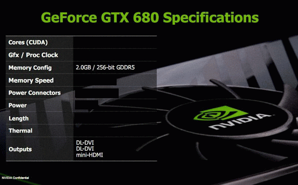


Bookmarks