

new internal bios in da house
this bios fixed an Q-Fan issue with R3E and has Gulftown improvements



new internal bios in da house
this bios fixed an Q-Fan issue with R3E and has Gulftown improvements


What does "has Gulftown improvements" mean?Originally Posted by Fire4Wire

This will be at least as fast as 878?
Heatware
Custom SS unit by Gray Mole, Sdumper Cascade, K|ngp|n F1 Gemnni, TEK9 Fatboy, TEK9 Slim, NB-1, H2O stuff...
Celeron 347, Celeron 356, Celeron 420, 2x P4 631, P4 670, P4 640, P4 651, P4 524, PD 915, P4 540J, 2x P4 530J, P4 520J Crucial Ballistix 2x1GB DDR2-8500 2x Asus REX X48, Gigabyte EP45-UD3P rev 1.0, Asus Commando P965,
Stuff I used to have:
Asus RIIIE X58, Evga Classified P55, Gigabyte EP45T-UD3LR, i5 670, E8600, Q9650, Q9550, , 3x2GB Mushkin Redline 2000C8,, G.Skill 2x2GB PC9600(Silver), Evga Evbot
XFX 4770 modded, XFX 7950GT, XFX 6600GT, Evga 8600GTS 512MB, 3850 OC, 4x 3870s, and X600
"In this world, Elwood, you must be oh so smart or oh so pleasant. Well, for years I was smart. I recommend pleasant." - James Stewart
No, those are the newer (PSC based I believe) kits. I have the Hyper MGH-E kit, CMG6GX3M3A2000C8 + extended fins.
Sure I don't mind. You have to know though that every cpu is different so voltages will vary. And if you are trying to stay on a 2:10 memory multi then you will need to hit atleast 200BCLK. And on top of all that, if you have two sets coming, I'm assuming you're trying to run 12gb. Expect to either run a lot of voltage to get them stable or run into problems. Key is to not try and skip ahead. Start from stock and you'll get a better understanding of what's going on. My settings are:
Code:Target CPU Frequency 3819MHz Target DRAM Frequency 2015MHz LN2 Mode: Disabled*** QPI Loadline Calibration: Enabled*** Sync Mode [Enabled] AI Overclock Tuner [Manual] OC From CPU level Up [Auto] CPU Ratio Setting [19.0] CPU Turbo Power Limit [Disabled] >CPU Configuration---------------------------- CPU Ratio Setting [19.0] C1E Support [Disabled] Hardware Prefetcher [Enabled] Adjacent Cache Line Prefetcher [Enabled] Intel(R) Virtualiyation Tech [Enabled] CPU TM Function [Disabled] Execute Disable Bit [Enabled] Intel(R) HT Technology [Enabled] Active Processor Cores [All] A20M [Disabled] Intel(R) SpeedStep(TM) Tech [Disabled] Intel(R) C-STATE Tech [Enabled] C State package limit setting [Auto] ---------------------------------------------- BCLK Frequency [201] PCIE Frequency [100] DRAM Frequency [2015] UCLK Frequency [4029] QPI Link Data Rate [7254] Memory Configuration Protect [Disabled] >DRAM Timing Control-------------------------- CAS# Latency 9 [7] RAS# to CAS# Delay 9 [7] RAS# PRE Time 9 [7] RAS# ACT Time 24 [20] RAS# to RAS# Delay 6 [AUTO] REF Cycle Time 110 [110] WRITE Recovery Time 15 [15] READ to PRE Time 9 [9] FOUR ACT WIN Time 31 [31] Back-To-BackCAS# Delay 0 [Auto] Timing Mode 1N [1N] Round Trip Latency on CHA [AUTO] Round Trip Latency on CHB [AUTO] Round Trip Latency on CHC [AUTO] WRITE To READ Delay(DD) 8 [Auto] WRITE To READ Delay(DR) 8 [Auto] WRITE To READ Delay(SR) 18 [Auto] READ To WRITE Delay(DD) 7 [Auto] READ To WRITE Delay(DR) 7 [Auto] READ To WRITE Delay(SR) 7 [Auto] READ To READ Delay(DD) 7 [Auto] READ To READ Delay(DR) 6 [Auto] READ To READ Delay(SR) 4 [Auto] WRITE To WRITE Delay(DD) 8 [Auto] WRITE To WRITE Delay(DR) 8 [Auto] WRITE To WRITE Delay(SR) 18 [Auto] ---------------------------------------------- CPU Differential Amplitude [Auto] CPU Clock Skew [Auto] IOH Clock Skew [Auto] ------------ Extreme Engine Digi+ ------------ Digi+ PWR Mode [T-Balanced] PWR Volt. Control [Auto] Load-Line Calibration [Full] CPU Voltege OCP [Enabled] CPU PWM Frequency [AUTO] Extreme OV [Disabled] Extreme OC [Auto] CPU Voltage 1.250 [1.13125] CPU PLL Voltage 1.812 [1.80200] QPI/DRAM Core Voltage 1.350 [1.36250] DRAM Bus Voltage 1.654 [1.65625] >DRAM REF Voltages---------------------------- DRAM DATA REF Voltage on CHA [+0mV] DRAM CTRL REF Voltage on CHA [+0mV] DRAM DATA REF Voltage on CHB [+0mV] DRAM CTRL REF Voltage on CHB [+0mV] DRAM DATA REF Voltage on CHC [+0mV] DRAM CTRL REF Voltage on CHC [+0mV] ---------------------------------------------- IOH Voltage 1.244 [1.11300] IOH PCIE Voltage 1.508 [1.51050] ICH Voltage 1.111 [1.11300] ICH PCIE Voltage [1.51050] ---------- Spread Spectrum Control ----------- CPU Spread Spectrum [Disabled] DRAM Spread Spectrum [Disabled] ***on-board jumper dependant
Yes, stock heatsinks, nothing wrong with them, they are very good looking.
But cooling them with 80mm fan @ 2400rpm, directly on top of them.
Maximus 5 Gene | i7-3770K @ 5GHz | ADATA 2x2GB @ 2.6GHz 9-12-10-28-1T | HD7970 @ 1200/6400
Rampage 4 Extreme | i7-3930K @ 5GHz ||| X58-A OC Orange | i7-980X @ 4.6GHz
Yea they are good looking but probably not as effective as say the Corsair or Kingston design, with the added direct air flow from the optional fan (available for kingston as well).
What kind of timings have you got out of them? I also have a set thats why I ask
Last edited by spoolindsm127; 08-19-2010 at 02:27 PM.
hum spoke too soon...i moved the gfx card from slot 2 to slot 1 and now it's unstable again. it was stable at 4.2 at only 1.3125 with 50% LLC, but now it's not stable even at 1.3250 with 50% LLC...weird. failing Linx after a few runs. anyone know if moving the gfx card would have affected things?
I posted the original message in this thread. Since I posted the message I've been through 3 further Rampage III Extreme boards for a total of 4 boards and all of them have malfunctioned!. The first 3 boards were connected to a PC Power & Cooling Turbo-Cool 1KW-SR 1000 watt PSU. I came to the conclusion that the PSU is defective and that's what is frying the boards. So I sent the PSU back to the manufacturer RMA and they sent me a refurbished one. The PC Power & Cooling technician that I talked to on the phone told me that they would test the unit that I returned to them and when I called a few days later to find out if the unit had tested defective they told me that the unit tested OK, There was nothing wrong with it. I still had suspicions about that PSU, Perhaps there was a incompatibility between this PSU and the motherboard because the Turbo-Cool 1KW-SR PSU is a 4 year old design . So I decided to buy a brand new Corsair HX1000 PSU which is on the Asus Qualified Vendors List (QVL) for 500 watt power supply and above that have been tested by Asus to work with this board, which is in the reference section in the back of the motherboard manual, Page A5.
I Paid $250 for it, but if it solves my problem I'll just keep going and not look back. When I got the 4th RMA RIIIE it tested ok outside and inside the case so I thought "At last, I've found the problem . So I just went ahead and started completing my build however I decided to power up just before I finished to make sure that everything installed so far was working properly and when I did NOTHING happened. The board wouldn't POST. i got the red light on the power on button on the board and the reset button light and in the back of the board in the I/O panel, the reset button light back there came on and on the bottom of the board the LED for the 1st BIOS came on after about 10 seconds. but no power to the CPU or fans so I'm sitting there scratching my heard trying to figure out what is wrong now. I decided that it must be the CPU although I really doubted that, I decided to RMA the CPU, an Intel I7 930 and try another one and when I got the replacement and tried it still nothing. I can't think of what else to try next.
I've tried 3 different PSU's two different CPU's. I only bench test with 1 memory module installed in the red socket closet to the CPU socket and both EPS12V power CPU Power lead connected and both EZ Molex plugs connected. I decided to send the board back to Asus in Fremont CA and let them figure out what is wrong with this motherboard. I didn't want another replacement, I just told them figure out what's wrong with the motherboard and send it back to me when it's fixed or send me a check for $429.00. The price I paid for it from Newegg.com. I have built many computers over the 15 years that I've been doing this but I have never had so many problems with a motherboard than I've had with this one. I'm a CompTIA A+ certified IT Technician but I'm stumped with this one. I'm about ready to pull the trigger on a EVGA Classified 3 way. I wish I didn't have to spend the extra money but I've already spent an extra $300 on top of what I paid for it just trying to get the Rampage III Extreme to work to no avail. Anybody got any ideas PLEASE let me know.
^^What kind of case do you have, or are you even running one? There are several reported cases of problems with certain cases, and even particular CPU heatsinks (i believe 1 of them was the VenomousX).
Sounds like its time to move on to something new, the Classified seems to be a great board. You have more patience than I would in that situation.
Corsair 800D Obsidian (Brand New) with Stock Intel Fan/Heatsink
Last edited by Coolbreeze; 08-19-2010 at 04:34 PM.
That 2.xx is coming from the BIOS. I run Linux on my box and see the 2.xx in the output from dmidecode
Code:Handle 0x0002, DMI type 2, 15 bytes Base Board Information Manufacturer: ASUSTeK Computer INC. Product Name: Rampage III Extreme Version: Rev 2.xx
Hi Guys
I'm hoping that someone can help me with what ought (I think) to be an elementary problem. I don't seem to be able to get my R3E/980X to run in turbo mode. I thought it was meant to work without having to do anything special but no matter what combination of BIOS settings I use, I seem to be stuck at a maximum of 3334MHz.
I'm using BIOS 9124 and running Linux, kernel 2.6.34, with a Core i7 980X on an R3E with 6 x 2GB RAM. I don't have access to the BIOS settings while typing this but I have tried various combinations of the Turbo Mode setting together with the two that the help on the right hand side of the screen say must be disabled (is it C1E and TM?).
I have no great wish to overclock but I would like to get turbo mode functional if at all possible. I check the speeds by running a single copy of `openssl speed` then
$ grep MHz /proc/cpuinfo
cpu MHz : 1600.000
cpu MHz : 1600.000
cpu MHz : 1600.000
cpu MHz : 1600.000
cpu MHz : 3334.000
cpu MHz : 1600.000
Is there some operating system dependency on turbo mode? I thought it was purely hardware and that using only a single core would boost it to 3.6GHz.
I have the board working fine in the Corsair case with both the PC Power & Cooling unit and the HX1000. Based on your description and that of your post at the ASUS forum talking about smoke or sparks I would venture to say that board is shorting out against something in the case. PM me your RMA case number and I will have someone contact you shortly about it.
Update -
Rampage III Extreme
Beta BIOS 0010 -
1. Fix Fan Ramp Issue with previous Beta
http://www.mediafire.com/file/c22yya...-ASUS-0010.rar
The only version out is 1.04G, there is not a 2.xxx version of the board. That number being reported is based on CPU Microcode. As far as one board clocking better than another one that is due to a whole host of factors but as far as the boards are concerned, the most important difference is the quality of the IOH. The difference between a really good IOH and an average one is easily worth 10 Bclk.
Not part of this but another myth is that the board is tuned more for Gulftown than Bloomfield and that is false. The BIOS microcode takes care of the base settings for either CPU. The difference is that each processor family requires different tuning methods to reach certain levels.
I have been contemplating whether to test out UD7 v2 and see how it does vs R3E for bloomfield since some people think RE3 is no good for none other than GT processors.
Overall I think the RE3 did quite well for 24/7 oc on my bloomfield
Here is my new board
This is REV.1.04G.
http://namegt.com/570

well i consider the rexIII not as good as a rexII for bloomfeild
not even close
both my classy 760 kickin its ass bigtime
i'll wait another week for a descent bloomfeild bios
hey Bingo any hope for bloomfeild?!!
i dont give a crap for subzero
i wonder if asus even cares
maximus IV extremegtx580
gigabut p67-ud7
p67 sabertooth
2500k+2600k
antec 1200watt
EVGA classified 760
920 Batch# 3849B018 4.985ghz@1.52vgtx285 ftw sli
OCZ3RPR1866LV6GK hypers
dfi ut p35
gigabut p35c-ds3r
gigabut x38-d6q
ballistix 85001240mhz@2.02v
asus cares
show me a good bloomfeild bios
i showed ya the $
maximus IV extreme
gigabut p67-ud7
p67 sabertooth
2500k+2600k
antec 1200watt
EVGA classified 760
920 Batch# 3849B018 4.985ghz@1.52v
OCZ3RPR1866LV6GK hypers
dfi ut p35
gigabut p35c-ds3r
gigabut x38-d6q
ballistix 8500
they all work and improving ...
when a rexIII not even close to a rexII for bloomfeild kinda ridiculous
ramapageII gene = rampage III extreme lol
Last edited by zsamz_; 08-19-2010 at 09:13 PM.
maximus IV extreme
gigabut p67-ud7
p67 sabertooth
2500k+2600k
antec 1200watt
EVGA classified 760
920 Batch# 3849B018 4.985ghz@1.52v
OCZ3RPR1866LV6GK hypers
dfi ut p35
gigabut p35c-ds3r
gigabut x38-d6q
ballistix 8500
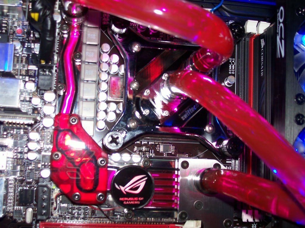
Corsair Obsidian Series 800D | ASUS Rampage III Extreme ( bios 901 ) | Intel Core i7-930 Bloomfield @4.0
| Full Custom WC | Corsair Dominator 6x2GB 1600 | Antec TPQ-1200 | 2 300 GB VelociRaptors | 2 580 GTX | Asus VW266h / W7 Ultimate 64bit
Don't hold out for a BIOS that makes Bloomfiled or Gulftown clock better. All of the factors that affect final clock speeds barring the basics of power delivery and memory sub-timings are automated (or in hardware, such as trace impedances), so the BIOS will not play a role in extending clocking margins past those factors at this point.
i got 3 920s here
1 will do 4.77 linx stable on rexII and e760
my best 920 maxed out 4.6 slow mode on rex IIIi even tried 3x1 hypers
i dont need extra special clocking bios just a bois that will function properly on bloomfeid i dont give a crap for gulftown i sold my chip
i dont a crap what the board will do zubzeroany cheap board will clock subzero
i'll even accept a bios as good as the rampage II gene
if we not gonna get a good bios for gulftown i'd like to know and just dump the board
maximus IV extreme
gigabut p67-ud7
p67 sabertooth
2500k+2600k
antec 1200watt
EVGA classified 760
920 Batch# 3849B018 4.985ghz@1.52v
OCZ3RPR1866LV6GK hypers
dfi ut p35
gigabut p35c-ds3r
gigabut x38-d6q
ballistix 8500


 Reply With Quote









Bookmarks