A very interesting point... did you test it on a similar board?
The overvoltage threshold is 250-350mV... the max VCore awailable in Bios is 1,7V... so all boards run into OVP arround 2V.
And you think, there is a pulldown resistor beetween FBRTN and GND?
But isnt it a bit risky to increase the ground voltage over 0V?
Because all other devices on the Board also use this reference 0V, so they can't work solid.
The only thing i could imagine:
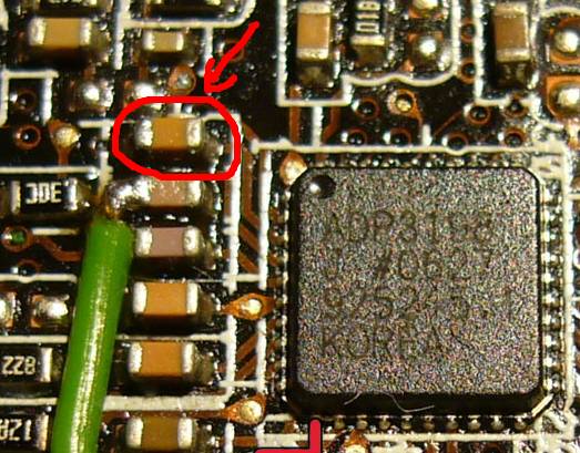
The ADP3198 uses a seperate ground and is single-point connected to GND, to keep noise back from the GND plane. This is most realized with a 0Ohm resistor. So we could remove this resistor and connect a stable power supply arround 50-100mV to the GND of the ADP3198 chip. This should give a a boost arround 50-100mV. But i believe there is no single-point connection in this case.
O how could we prevent, to increase the GND level of the whole system/board?
Can we cut the track to pin 3 and solder instead of this track a stable 100mV power supply?
Thank you very much!
I hope you understand my bad english

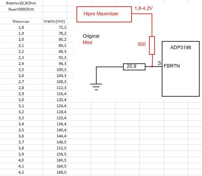
PS: so the idea is, to solder a 50k VR from 3,3V to the ADP3198, not to pin 11 (as done before), but to pin 3... right?


At first pic:


 Reply With Quote


 But it would be nice, if someone can test that
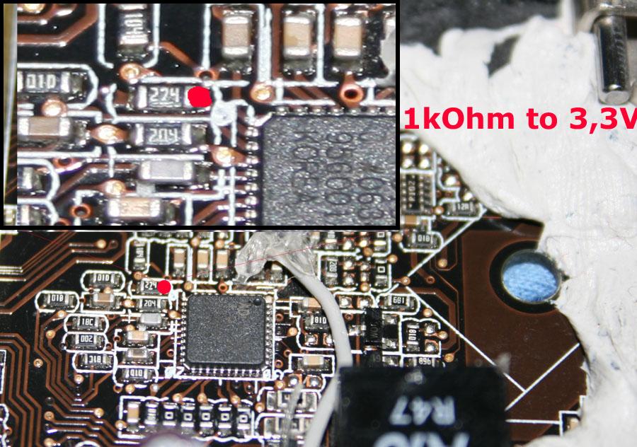


Bookmarks