

Just a fan on themOriginally Posted by CoolZone


Just a fan on them
How I fixed: I placed 5 1in binder on them then let a overnight Memtest #5 on tight timmings and high speed.
Now with the tape re-glued by the heat I only need 2 binders on each module and it will fit the 4 sticks without touching each other.
All with active cooling (OCZ XTC).
Fixed:

//RETIRED-o00o--°(_)°--o00o-OVERCLOCKER//

Sorry to be a pain, but I was hoping someone could answer my question regarding a vCore limit to the 45nm Quads ... in my case the Xeon 3360 ...
I am slowly working into this board and proc with 4GB OCZ Reaper PC2 8500. I can't quite seem to get a decent range of voltages that will let me go above 445FSB with either the 8 or 8.5 multi ... any suggestions? At 440 FSB with the 8.5 multi, and vCore around 1.36v she'll boot into Windows (XP 64) without a hitch, but as soon as I try to run Prime95, the first two cores halt immediately , yet the second two keep on working ... really weird shyt! I can bring it back down to stock volts and not a single problem with all four cores ...
Intel i7 7700K @ 5.1 GHz w/Corsair H115i * ASUS Maximus Hero IX* BIOS 0701 * 32GB Corsair Vengeance DDR4 3200MHz * 2 x 256GB Samsung 950 Pro NVMe (RAID 0) * 1TB Samsung 850 Pro (Steam Drive) * 4TB WD Green (Storage) * Corsair HX1000i * Corsair 750D Obsidian Airflow Edition

Those Prime95 issues can be due to wrong GTL settings or disabled.
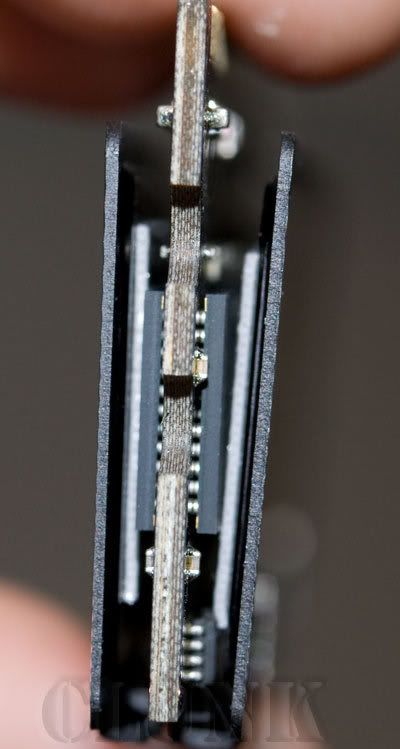
Did you try to tweak GTL'S acording to Cluncks chart?
It's not always vcore that your processor is asking for.
//RETIRED-o00o--°(_)°--o00o-OVERCLOCKER//
I have been working with them today ... I started all over from scratch and now I am in a Prime run with settings as follows: vCore-1.26v(real 1.24v); CPU VTT-1.1v(same); NB-1.462v(real 1.45v); DRAM-2.19v(real 2.16v); 8.5 multi x 400 FSB, DRAM Target speed is 333/800, GTL is disabled for the time being ...
I have had it up higher and did some preliminary benching with SuperPi but what is the fault when the error says "NOT IN ROUND" or "NOT IN CONVERGENCE" or something to that effect? Do I need more or less of whatever?
Intel i7 7700K @ 5.1 GHz w/Corsair H115i * ASUS Maximus Hero IX* BIOS 0701 * 32GB Corsair Vengeance DDR4 3200MHz * 2 x 256GB Samsung 950 Pro NVMe (RAID 0) * 1TB Samsung 850 Pro (Steam Drive) * 4TB WD Green (Storage) * Corsair HX1000i * Corsair 750D Obsidian Airflow Edition
thanks, now im really worried lol
i checked them they dont look like there pealing yet. and they seemed stable with all 4 at 1140mhz . but then today i got the c1 error and it wouldnt boot , i restarted and it boot ok. so im getting worried. and im too scared to run a memtest on them incase i get bad results. lol
system 1 -
ltx48t2r / E8500/485fsb / mushkins 2x2gb/ gtx280/ 150gb velociraptor /tagan 1100w psu/watercooled
/vista 64
system 2-
biostar i45/ xeon 3360 3.8ghz 450fsb/gtx280/ 3x74gb raptors raid0/crucial ballistix 2x1gb 1080mhz /thermaltake tp 850w/water cooled/xp gamers edition
Silly question, are the green and yellow board connectors UV reactive?
i7 3770k <> ASUS P8Z77-V Deluxe <> Windows 7 Ultimate 64-bit SP1
4 X 4GB Samsung MV-3V4G3D/US <> Corsair H100
EVGA GTX 580 w/ AXP+VR004 <> X-Fi Titanium HD <> ASUS VG236H <> Senn 598
Intel 520 240GB, WD Blacks x 3, Corsair Force 3 60GB (caching) <> Pioneer BDR-203BKS
Seasonic Platinum 860 <> Corsair 600T SE <> Logitech G700 <> Logitech G19 keyboard
If X48 is like X38, then memory clocks maybe sensitive to clock fine delay values once oc'd - might want to fine tune the values for your memory http://i4memory.com/showthread.php?t=4743 which can product very dramatic gains in some cases!
---
thanks eva thats awsome info there. ill read through it soon and get into changing some of those fine tune settings. i did notice fine tune in bios before but wasnt sure what i should set them to.
thanks again.
system 1 -
ltx48t2r / E8500/485fsb / mushkins 2x2gb/ gtx280/ 150gb velociraptor /tagan 1100w psu/watercooled
/vista 64
system 2-
biostar i45/ xeon 3360 3.8ghz 450fsb/gtx280/ 3x74gb raptors raid0/crucial ballistix 2x1gb 1080mhz /thermaltake tp 850w/water cooled/xp gamers edition

Greetings all,
Can't seem to get my X48, Q6600, or G.Skill PC28000 2gbx2 stable at anything past 3.6 on 333/800, or anything reasonable on 333/677. I know the chip can boot into windows at 4.2, and the memory clocks to around 1030. Would I use 333/667? When I do get anything remotely stable, I have corruption on downloads and random crashes in small applications (Firefox, pidgin), but they can OCCT for 30 min+.
Here are my current settings I'm using to achieve 3.6 barely stable.
Any help appreciated, as I have a sweet WC setup and want to hit 4Code:CPU Feature Page Thermal Management Control................Disabled PPM (EIST) Mode...........................Disabled Limit CPUID MaxVal........................Disabled CIE Function..............................Disabled Execute Disable Bit.......................Disabled Virtualization Technology.................Disabled Core Multi-Processing.....................Enabled Main BIOS Page Exist Setup Shutdown......................Mode 1 Shutdown After AC Loss....................Enabled O. C. Fail Retry Counter..................0 CLOCK VC0 Divider.........................Auto CPU Clock Ratio...........................8x CPU Clock.................................450 MHz Boot Up Clock.............................Auto DRAM Speed................................333/800 PCIE Clock................................100 MHz PCIE Slot Config..........................1X 1X CPU Spread Spectrum.......................Disabled PCIE Spread Spectrum......................Disabled SATA Spread Spectrum......................Disabled Voltage Setting Page CPU VID Control...........................1.4V CPU VID Special Add.......................Auto DRAM Voltage Control......................2.1V SB Core/CPU PLL Voltage...................1.510V NB Core Voltage...........................1.504V CPU VTT Voltage...........................1.327V VCore Droop Control.......................Enabled Clockgen Voltage Control..................3.45V GTL+ Buffers Strength.....................Strong Host Slew Rate............................Weak GTL REF Voltage Control...................Disabled CPU GTL1/3 REF Volt.......................N/A CPU GTL 0/2 REF Volt......................N/A North Bridge GTL REF Volt ................N/A DRAM Timing Page Enhance Data Transmitting.................Fast Enhance Addressing........................Fast T2 Dispatch...............................Enabled Clock Setting Fine Delay..................Listed Below CAS Latency Time (tCL)....................5 RAS# to CAS# Delay (tRCD).................5 RAS# Precharge (tRP)......................3 Precharge Delay (tRAS)....................15 All Precharge to Act......................4 REF to ACT Delay (tRFC)...................48 Performance Level.........................8 Read Delay Phase Adjust...................Listed Below MCH ODT Latency...........................2 Write to PRE Delay (tWR)..................14 Rank Write to Read (tWTR).................11 ACT to ACT Delay (tRRD)...................3 Read to Write Delay (tRDWR)...............8 Ranks Write to Write (tWRWR)..............4 Ranks Read to Read (tRDRD)................5 Ranks Write to Read (tWRRD)...............4 Read CAS# Precharge (tRTP)................3 ALL PRE to Refresh........................4 Read Delay Phase Adjust Page Channel 1 Phase 0 Pull-In.................Enabled Channel 1 Phase 1 Pull-In.................Enabled Channel 1 Phase 2 Pull-In.................Enabled Channel 1 Phase 3 Pull-In.................Enabled Channel 1 Phase 4 Pull-In.................Enabled Channel 2 Phase 0 Pull-In.................Enabled Channel 2 Phase 1 Pull-In.................Auto Channel 2 Phase 2 Pull-In.................Enabled Channel 2 Phase 3 Pull-In.................Enabled Channel 2 Phase 4 Pull-In.................Enabled Clock Setting Fine Delay Page Ch1 Clock Crossing Setting................More Aggressive DIMM 1 Clock fine delay...................Current 89ps DIMM 2 Clock fine delay...................Current 456ps DIMM 1 Control fine delay.................Current 534ps DIMM 2 Control fine delay.................Current 289ps Ch 1 Command fine delay...................Current 801ps Ch2 Clock Crossing Setting................More Aggressive DIMM 3 Clock fine delay...................Current 89ps DIMM 4 Clock fine delay...................Current 400ps DIMM 3 Control fine delay.................Current 367ps DIMM 4 Control fine delay.................Current 356ps Ch 2 Command fine delay...................Current 801ps Ch1Ch2 CommonClock Setting................More Aggressive Ch1 RDCAS GNT-Chip Delay..................Auto Ch1 WRCAS GNT-Chip Delay..................Auto Ch1 Command to CS Delay...................Auto Ch2 RDCAS GNT-Chip Delay..................Auto Ch2 WRCAS GNT-Chip Delay..................Auto Ch2 Command to CS Delay...................Auto
edit: I also have tinkered a bit with gtls, and maybe that was one of the reasons I hit 4.2 and posted one time. Any recommendations for 4.0-4.2ghz gtls and corresponding vtt?
double edit: I am no longer even stable at 3.6 for long periods, ater a while I get app crashes then bsod.
Last edited by Rinaun; 04-19-2008 at 04:55 AM.
I just checked im my blue led case, and I didn't see much glow off of the sata plugins. Everything else lights up I think.
I just got all my new parts up and running but i keep getting random system freezes while playing games (Pro Street, Supreme Commander).
Running XP 32, 8.2 Catalyst. Rest is in signature. Not to sure if its related to voltage settings in the bios. Even with everything at the defaults in the Bios it still freezes.
Any help would be great.
Intel Q6600, 400x9 @ 1.5v, TRUE Black
DFI Lanparty X48
OCZ SLI Ready 2 x 2gb DDR-800
Force 3D 4870X2
Antec 1200
G15 Rev.1 + Razer Lachesis
Samsung 245T 24"
Sennheiser HD 485
Logitech Z5500 5.1
Have you run 3dmark 06 yet ??
ASUS RANGER VII
i7 4790K
8GB CORSAIR 1600 xmp
BE QUIET SHADOWROCK SR1
EVGA GTX 770
2 X 840 EVO SSD
CORSAIR AX850W
Yeah i did. Multiple times. Supposedly there is a compatibility issue with DFI X38 and 3870X2. Guess the problem was brought accross to the X48. Anyone know of a sure fire fix for this?
Intel Q6600, 400x9 @ 1.5v, TRUE Black
DFI Lanparty X48
OCZ SLI Ready 2 x 2gb DDR-800
Force 3D 4870X2
Antec 1200
G15 Rev.1 + Razer Lachesis
Samsung 245T 24"
Sennheiser HD 485
Logitech Z5500 5.1
eva, ive been reading through that link,( since i just discovered im not occt stable).
my question is wouldnt setting fine delay to relaxed have the same effect? or am i better of reducing memory speed abit then reseting fine delay to match stable settings?
edit* relaxed settings didnt do anything, so forget that q's . still unstable with occt. im trying what u said and i reduced my memory speed. but i had to reduce fsb to reduce memory speed. how can i reduce memory speed only? it doesnt seem to have a separate setting for reducing memory speed? i overclocked using strap settings and increasing fsb i didnt increase memory manually.
also is occt to strict? seems stable with prime but looses out with occt.
Last edited by adya; 04-19-2008 at 06:59 PM.
system 1 -
ltx48t2r / E8500/485fsb / mushkins 2x2gb/ gtx280/ 150gb velociraptor /tagan 1100w psu/watercooled
/vista 64
system 2-
biostar i45/ xeon 3360 3.8ghz 450fsb/gtx280/ 3x74gb raptors raid0/crucial ballistix 2x1gb 1080mhz /thermaltake tp 850w/water cooled/xp gamers edition
For OCing and WCing, is it ok to stick with the stock SB heatsink? I'd expect so, since if I recall what I read somewhere, 2 of the things the SB is responsible for is the JMicron and the on-board sound, neither of which I'll be using I expect, plus that high intake fan on the TJ09 will probably put air right on it. I'm just in planning to order parts mode and wanted to see if I needed to snag something like an Enzotech SLF-1.
i7 3770k <> ASUS P8Z77-V Deluxe <> Windows 7 Ultimate 64-bit SP1
4 X 4GB Samsung MV-3V4G3D/US <> Corsair H100
EVGA GTX 580 w/ AXP+VR004 <> X-Fi Titanium HD <> ASUS VG236H <> Senn 598
Intel 520 240GB, WD Blacks x 3, Corsair Force 3 60GB (caching) <> Pioneer BDR-203BKS
Seasonic Platinum 860 <> Corsair 600T SE <> Logitech G700 <> Logitech G19 keyboard
SB heatsink works well, doesn't really get very hot.
Can't hurt to give it a repaste though
i reduced my fsb/memory to 450/1080 ive been running occt for 1 1/2 hours seems stable , so ill go into bios when its finished and note down fine delay settings. then increase fsb/memory back to 475/1140 with stable fine delay setting on manual.
edit* ok i did it , but the stable "current" settings wont match the manual settings? sometimes by more than 50. i had to use the closest figure. any way of setting it to the exact figure?
Last edited by adya; 04-19-2008 at 08:09 PM. Reason: stuff
system 1 -
ltx48t2r / E8500/485fsb / mushkins 2x2gb/ gtx280/ 150gb velociraptor /tagan 1100w psu/watercooled
/vista 64
system 2-
biostar i45/ xeon 3360 3.8ghz 450fsb/gtx280/ 3x74gb raptors raid0/crucial ballistix 2x1gb 1080mhz /thermaltake tp 850w/water cooled/xp gamers edition
damn i cant get it stable at 475/1141 . becuase i cant set fine delay to the exact stable settings.
is it better to just keep lowering it till its stable? lower= stable? its a shame this bios wont allow me to set it manually properly.
system 1 -
ltx48t2r / E8500/485fsb / mushkins 2x2gb/ gtx280/ 150gb velociraptor /tagan 1100w psu/watercooled
/vista 64
system 2-
biostar i45/ xeon 3360 3.8ghz 450fsb/gtx280/ 3x74gb raptors raid0/crucial ballistix 2x1gb 1080mhz /thermaltake tp 850w/water cooled/xp gamers edition
I just ran prime95 for 11 hours straight with my q6600,
9x420 = 3780MHz
strap 400/800
vcore 1.392v
VTT 1,312v
NB 1.504v
And now I installed another 4 gigs of ram, let's see how high I can go with 8gb
Q6600 (IHS removed) @ 3600 MHz 1.408v
DFI LanParty LT x48-T2R (1224 LT ICH9R modded bios)
4 GB Transcend Jetram @ 400 MHz 5-5-5-16 2T 1.872v
Sapphire HD4850x2 710 / 1075 MHz
PC-Power & Cooling Turbo-Cool 1kW PSU
2* OCZ Vertex2 extended 60GB @ raid0 @ ICH9R
5* Seagate 7200.11 1.5TB @ raid5 @ Promise EX8350 PCI-e RAID card
Dimastech Easy v2.5 bench table
DELL 3008WFP 30" + 2* Eizo Flexscan L887 20,1" (pivot)
Windows 7 x64
CPU EK Supreme Acetal LT | NB Swiftech MCW30 | GPU 2* Swiftech MCW60 | PUMP Phobya 400 | RAD DIY monster outside the house | TUBING 1/2" ID
mines prime stable for 5 hours but fails with occt. i think occt is either way to strict with its testing or prime is weak. has to be one or the other.
did u test with occt at all?
system 1 -
ltx48t2r / E8500/485fsb / mushkins 2x2gb/ gtx280/ 150gb velociraptor /tagan 1100w psu/watercooled
/vista 64
system 2-
biostar i45/ xeon 3360 3.8ghz 450fsb/gtx280/ 3x74gb raptors raid0/crucial ballistix 2x1gb 1080mhz /thermaltake tp 850w/water cooled/xp gamers edition
damn lol i dont test prime more than 1 hour no more
puts too much stress on components for my taste
9 hours i bet you stable
maximus IV extreme
gigabut p67-ud7
p67 sabertooth
2500k+2600k
antec 1200watt
EVGA classified 760
920 Batch# 3849B018 4.985ghz@1.52v
OCZ3RPR1866LV6GK hypers
dfi ut p35
gigabut p35c-ds3r
gigabut x38-d6q
ballistix 85001240mhz@2.02v
Nope, I use just prime.
425fsb gives a BSOD within 30 minutes. If the CPU isn't getting enough juice, shouldn't the prime worker threads just halt to an error? So, is this a memory/NB -related issue?
Q6600 (IHS removed) @ 3600 MHz 1.408v
DFI LanParty LT x48-T2R (1224 LT ICH9R modded bios)
4 GB Transcend Jetram @ 400 MHz 5-5-5-16 2T 1.872v
Sapphire HD4850x2 710 / 1075 MHz
PC-Power & Cooling Turbo-Cool 1kW PSU
2* OCZ Vertex2 extended 60GB @ raid0 @ ICH9R
5* Seagate 7200.11 1.5TB @ raid5 @ Promise EX8350 PCI-e RAID card
Dimastech Easy v2.5 bench table
DELL 3008WFP 30" + 2* Eizo Flexscan L887 20,1" (pivot)
Windows 7 x64
CPU EK Supreme Acetal LT | NB Swiftech MCW30 | GPU 2* Swiftech MCW60 | PUMP Phobya 400 | RAD DIY monster outside the house | TUBING 1/2" ID
test with memtest to see if its memory related
try 1.45cpu n 1.4 cpuvtt try setting correct glt settings
4 sticks you ganna need 1.5v++on nb
maximus IV extreme
gigabut p67-ud7
p67 sabertooth
2500k+2600k
antec 1200watt
EVGA classified 760
920 Batch# 3849B018 4.985ghz@1.52v
OCZ3RPR1866LV6GK hypers
dfi ut p35
gigabut p35c-ds3r
gigabut x38-d6q
ballistix 8500
@zsamz_ - How did you put the X48 BIOS on your DFI X38 board?
 Posting Permissions


 Reply With Quote

Bookmarks