

Edit: Looks like these chips will be available in Q3 2017 from the presentation.Specs:
- 815mm2 die
- 12nm FinFet
- 21B Transistors
- 15 FP32 TFLOPS
- 7.5 FP64 TFLOPS
- NEW 120 Tensor TFLOPS
- 16GB HBM2 @ 900 GB/s
- 5120 CUDA cores
Link to full article


Edit: Looks like these chips will be available in Q3 2017 from the presentation.Specs:
- 815mm2 die
- 12nm FinFet
- 21B Transistors
- 15 FP32 TFLOPS
- 7.5 FP64 TFLOPS
- NEW 120 Tensor TFLOPS
- 16GB HBM2 @ 900 GB/s
- 5120 CUDA cores
Link to full article
Last edited by EternityZX9; 05-10-2017 at 01:12 PM.
Intel Core i7 7700K | MSI Z270 XPOWER G.T. | EVGA 1080Ti SC2 | 16GB DDR4 G.Skill Trident Z 3200 | Samsung S27A950D | 3 x Samsung 850 EVO (250GB, 2 x 2TB) | EVGA Supernova P2 1200w | Coolermaster Cosmos II
That's a ton of float point processing power....
Again, AMD's silence on Vega is deafening.
Originally Posted by Hans de Vries

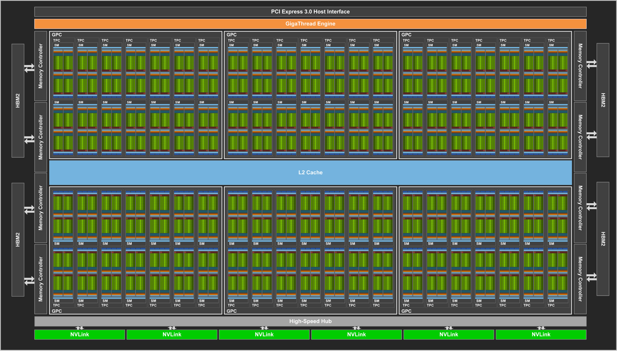
NVIDIA Volta GV100 GPU Key Features:
Key compute features of the NVIDIA Volta GV100 based Tesla V100 include the following:
- New Streaming Multiprocessor (SM) Architecture Optimized for Deep Learning Volta features a major new redesign of the SM processor architecture that is at the center of the GPU. The new Volta SM is 50% more energy efficient than the previous generation Pascal design, enabling major boosts in FP32 and FP64 performance in the same power envelope. New Tensor Cores designed specifically for deep learning deliver up to 12x higher peak TFLOPs for training. With independent, parallel integer and floating point datapaths, the Volta SM is also much more efficient on workloads with a mix of computation and addressing calculations. Volta?s new independent thread scheduling capability enables finer-grain synchronization and cooperation between parallel threads. Finally, a new combined L1 Data Cache and Shared Memory subsystem significantly improves performance while also simplifying programming.
- Second-Generation NVLink The second generation of NVIDIA?s NVLink high-speed interconnect delivers higher bandwidth, more links, and improved scalability for multi-GPU and multi-GPU/CPU system configurations. GV100 supports up to 6 NVLink links at 25 GB/s for a total of 300 GB/s. NVLink now supports CPU mastering and cache coherence capabilities with IBM Power 9 CPU-based servers. The new NVIDIA DGX-1 with V100 AI supercomputer uses NVLink to deliver greater scalability for ultra-fast deep learning training.
- HBM2 Memory: Faster, Higher Efficiency Volta?s highly tuned 16GB HBM2 memory subsystem delivers 900 GB/sec peak memory bandwidth. The combination of both a new generation HBM2 memory from Samsung, and a new generation memory controller in Volta, provides 1.5x delivered memory bandwidth versus Pascal GP100 and greater than 95% memory bandwidth efficiency running many workloads.
- Volta Multi-Process Service Volta Multi-Process Service (MPS) is a new feature of the Volta GV100 architecture providing hardware acceleration of critical components of the CUDA MPS server, enabling improved performance, isolation, and better quality of service (QoS) for multiple compute applications sharing the GPU. Volta MPS also triples the maximum number of MPS clients from 16 on Pascal to 48 on Volta.
- Enhanced Unified Memory and Address Translation Services GV100 Unified Memory technology in Volta GV100 includes new access counters to allow more accurate migration of memory pages to the processor that accesses the pages most frequently, improving efficiency for accessing memory ranges shared between processors. On IBM Power platforms, new Address Translation Services (ATS) support allows the GPU to access the CPU?s page tables directly.
- Cooperative Groups and New Cooperative Launch APIs Cooperative Groups is a new programming model introduced in CUDA 9 for organizing groups of communicating threads. Cooperative Groups allows developers to express the granularity at which threads are communicating, helping them to express richer, more efficient parallel decompositions. Basic Cooperative Groups functionality is supported on all NVIDIA GPUs since Kepler. Pascal and Volta include support for new Cooperative Launch APIs that support synchronization amongst CUDA thread blocks. Volta adds support for new synchronization patterns.
- Maximum Performance and Maximum Efficiency Modes In Maximum Performance mode, the Tesla V100 accelerator will operate unconstrained up to its TDP (Thermal Design Power) level of 300W to accelerate applications that require the fastest computational speed and highest data throughput. Maximum Efficiency Mode allows data center managers to tune power usage of their Tesla V100 accelerators to operate with optimal performance per watt. A not-to-exceed power cap can be set across all GPUs in a rack, reducing power consumption dramatically, while still obtaining excellent rack performance.
- Volta Optimized Software New versions of deep learning frameworks such as Caffe2, MXNet, CNTK, TensorFlow, and others harness the performance of Volta to deliver dramatically faster training times and higher multi-node training performance. Volta-optimized versions of GPU accelerated libraries such as cuDNN, cuBLAS, and TensorRT leverage the new features of the Volta GV100 architecture to deliver higher performance for both deep learning and High Performance Computing (HPC) applications. The NVIDIA CUDA Toolkit version 9.0 includes new APIs and support for Volta features to provide even easier programmability.
Intel Core i7 7700K | MSI Z270 XPOWER G.T. | EVGA 1080Ti SC2 | 16GB DDR4 G.Skill Trident Z 3200 | Samsung S27A950D | 3 x Samsung 850 EVO (250GB, 2 x 2TB) | EVGA Supernova P2 1200w | Coolermaster Cosmos II
Impressive performance and die size. Probably still >1 year until a similar chip trickles down to the x80 Ti series, but intriguing nonetheless. I don't even want to think about what yields will be on a 12nm chip that big though.
If I had to guess, on the gaming side of products release dates:
2080 GTX Volta in March 2018
Volta Titan sometime between May to August 2018
Volta Ti in March 2019.
Something like that.
Intel Core i7 7700K | MSI Z270 XPOWER G.T. | EVGA 1080Ti SC2 | 16GB DDR4 G.Skill Trident Z 3200 | Samsung S27A950D | 3 x Samsung 850 EVO (250GB, 2 x 2TB) | EVGA Supernova P2 1200w | Coolermaster Cosmos II
What about Volta Titan 2.0?
Intel 8700k
16GB
Asus z370 Prime
1080 Ti
x2 Samsung 850Evo 500GB
x 1 500 Samsung 860Evo NVME
Swiftech Apogee XL2
Swiftech MCP35X x2
Full Cover GPU blocks
360 x1, 280 x1, 240 x1, 120 x1 Radiators

https://www.techpowerup.com/233198/n...licon-detailed
NVIDIA at the GTC 2017 event, announced its next-generation "Volta" GPU architecture. As with its current "Pascal" architecture, "Volta" was unveiled in its biggest, most feature-rich implementation, the Tesla V100 HPC board, driven by the GV100 silicon. Given the HPC applications of NVIDIA's Tesla family of products, the GV100 has certain components that won't make it to the consumer GeForce family. Despite these, the GV100 is the pinnacle of NVIDIA's silicon engineering. According to the GPU block diagram released by the company, the GV100 has a similar component hierarchy to previous-generation NVIDIA chips, with some major changes to its basic number-crunching machinery, the streaming multiprocessor (SM).
The "Volta" streaming multiprocessor (SM) on the GV100 silicon features both FP32 and FP64 CUDA cores. Consumer graphics implementations of "Volta" which drive future GeForce products could lack those specialized FP64 cores. Each SM features 64 FP32 CUDA cores, and 32 FP64 cores. The FP64 cores can handle 32-bit, 16-bit, and even primitive 8-bit operations. The GV100 features 80 SMs, so you're looking at 5,120 FP32 and 2,560 FP64 CUDA cores. In addition, Volta introduces a component called Tensor cores, specialized machinery designed to speed up deep-learning training and neural net building. An SM has 8 of these, so the GV100 has 640. As with FP64 cores, Tensor cores may not make it to consumer-graphics implementations. Given its SM count, the GV100 features 320 TMUs. NVIDIA clocked the GV100 to run at 1455 MHz boost.

 Posting Permissions


 Reply With Quote
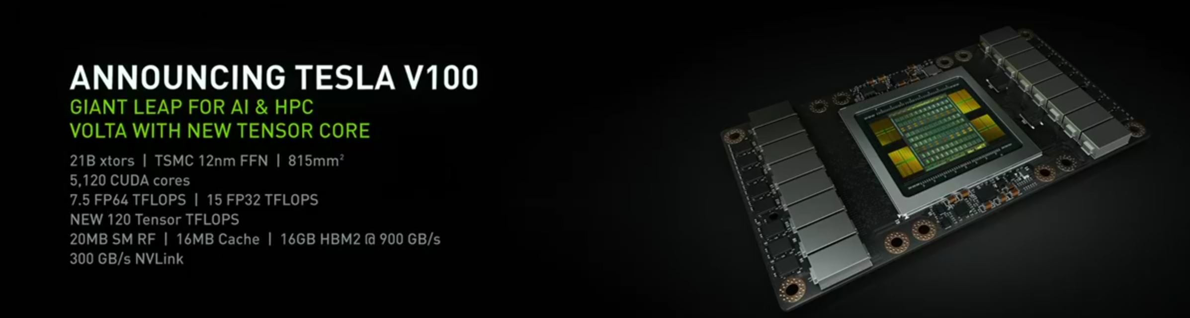


Bookmarks