Results 1 to 5 of 5

Thread: [News] Rambus outlines HBM3 and DDR5 specs in investor meeting

  1. #1
    Join XS BOINC Team StyM's Avatar
    Join Date
    Mar 2006
    Location
    Tropics
    Posts
    9,468

    [News] Rambus outlines HBM3 and DDR5 specs in investor meeting

    http://hexus.net/tech/news/ram/11309...estor-meeting/

    We have only mentioned HBM3 once before in the HEXUS news. The next gen high bandwidth memory technology was touched upon in presentations by Samsung and SK hynix at the Hot Chips Symposium last year. At that time we learned that HBM3 would improve on density, bandwidth, cost, and power consumption and it was hoped it would be widely welcomed by a range of industries from high performance computing and servers, to graphics, networking and many more.

    Though no hard figures were projected last year, Samsung's HBM3 presentation did indicate that HBM3 density would be 2x or better, peak bandwidth would be 2x or better and IO/Core voltage would be "much less", compared to HBM2.

    Now we have some more refined figures for HBM3 from Rambus. The data was shown to investors at a company event earlier this week. By all indications the release of HBM3 product is quite a way off so keep in mind that specs might change before this third gen HBM materialises.

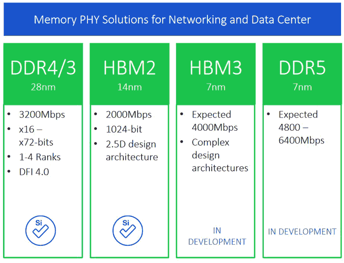
    The key slide from the Rambus event is reproduced above, and came via ComputerBase. You can see that, as indicated a year back, the expected bandwidth of HBM3 is 4000Mbps. Rambus also signals that the design complexity goes up. HBM2 used a 2.5D architecture and with HBM3 the stack height is increased.

    The only other data of note from the Rambus presentation slide is that HBM3 will be made on the 7nm node. It isn't expected that we will see 7nm semiconductor products until 2019 at the earliest.

    Rambus also mentioned DDR5 on two of its slides. In the first slide, sitting alongside the HBM3 in development box you can see DDR5 mentioned. The key info here is that DDR5 will deliver an expected bandwidth of 4800 - 6400Mbps. Like HBM3, it is set to be fabricated at 7nm.


  2. #2
    Xtreme Enthusiast
    Join Date
    Feb 2010
    Posts
    578
    To hell with RAMBUS. To hell with all of them, forever.

    Tell them to get their filthy hands off HBM.

  3. #3
    Xtreme Addict
    Join Date
    Dec 2004
    Location
    Flying through Space, with armoire, Armoire of INVINCIBILATAAAAY!
    Posts
    1,939
    Well, nobody else feels like putting much effort into developing new memory technologies. Sure, they're patent trolls - but the DRAMurai are also notorious for trying to dodge royalty/license fee payment. The reality is every company is a greedy rear end.
    Sigs are obnoxious.

  4. #4
    Xtreme Mentor
    Join Date
    Apr 2003
    Location
    Ankara Turkey
    Posts
    2,631
    Complex design architectures!!! Is this a good thing?


    When i'm being paid i always do my job through.

  5. #5
    Xtreme Enthusiast
    Join Date
    Feb 2010
    Posts
    578
    Quote Originally Posted by iddqd View Post
    Well, nobody else feels like putting much effort into developing new memory technologies.
    HBM is supposed to be Hynix's baby. Well Hynix + AMD.

    Sure, they're patent trolls - but the DRAMurai are also notorious for trying to dodge royalty/license fee payment. The reality is every company is a greedy rear end.
    JEDEC members typically steal from one another and then jockey to produce the best products they can from the patents utilized in common among the members. The only issue I have with any of them as a consumer is the price fixing.

Bookmarks

Bookmarks

Posting Permissions

  • You may not post new threads
  • You may not post replies
  • You may not post attachments
  • You may not edit your posts
  •