Results 1 to 4 of 4

Thread: [News] AMD's Ryzen Chips 10% Smaller Than Comparable Intel Skylake Dies

  1. #1
    Join XS BOINC Team StyM's Avatar
    Join Date
    Mar 2006
    Location
    Tropics
    Posts
    9,468

    [News] AMD's Ryzen Chips 10% Smaller Than Comparable Intel Skylake Dies

    https://www.techpowerup.com/230446/a...l-skylake-dies

    At the International Solid State Circuits Conference (ISSCC), AMD presented a whitepaper in which they demonstrated how its upcoming Zen x86 core fits into a 10 percent smaller die area than Intel's currently shipping second-generation 14nm processor. According to reports, analysts and Intel engineers in the session said the Zen core is clearly competitive, though many as-of-yet unknown variables will determine whether the die advantage translates into lower costs for AMD. That said, one thing is clear: the chip will have to perform in addition to being smaller, if AMD wants to ever capitalize on the potentially higher margins a smaller die could grant them.

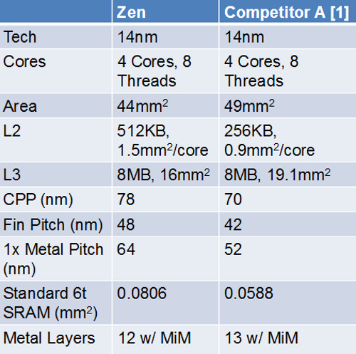
    One of the ways AMD improved upon its ZEN core in comparison to its previous products has been on switching capacitance for their new chips, with a reported overall 15% improvement. In addition, AMD has apparently moved on to a metal-insulator-metal capacitor design, thus achieving lower operating voltages as well as as more fine-grained per-core voltage and frequency control (on to become part of their SenseMI technology suite). Looking at the image, which pits an AMD ZEN chip to a comparable Intel solution, we see that AMD saves additional die space by making do with only 12 metal layers as well as overall lower L2 and L3 cache footprints.


  2. #2
    Xtreme Mentor
    Join Date
    Nov 2005
    Location
    Devon
    Posts
    3,437
    This table shows how much better Intel process really is in the real world.
    Despite SRAM cell size deficit somehow AMD engineers managed to create smaller overlay cache sizes. Of course cache includes a lot of supporting circuity and one could say it is there where AMD made it's savings.

    I'm looking forward to the launch and hope for competitive product at a reasonable price which will offer performance good enough for excuse to upgrade from i7 4790K
    RiG1: Ryzen 7 1700 @4.0GHz 1.39V, Asus X370 Prime, G.Skill RipJaws 2x8GB 3200MHz CL14 Samsung B-die, TuL Vega 56 Stock, Samsung SS805 100GB SLC SDD (OS Drive) + 512GB Evo 850 SSD (2nd OS Drive) + 3TB Seagate + 1TB Seagate, BeQuiet PowerZone 1000W

    RiG2: HTPC AMD A10-7850K APU, 2x8GB Kingstone HyperX 2400C12, AsRock FM2A88M Extreme4+, 128GB SSD + 640GB Samsung 7200, LG Blu-ray Recorder, Thermaltake BACH, Hiper 4M880 880W PSU

    SmartPhone Samsung Galaxy S7 EDGE
    XBONE paired with 55'' Samsung LED 3D TV

  3. #3
    Xtreme Enthusiast
    Join Date
    Oct 2012
    Posts
    687
    Im not sure there is something to be really proud of.
    Yes they packed it denser, while using one less metal layer.That could be the reason why it clocks lower...
    AMD on their first attempt tends to go too optimistic, and later on they have to fix it.
    Intel 5960X@4.2Ghz[Prime stable]@4.5 [XTU stable] 1.24v NB@3.6ghz Asrock X99 Extreme 3 4x8GB Corsair Vengeance@3200 16-17-17
    Sapphire nitro+ VEGA 56 Samsung SSD 850 256GB Crucial MX100 512GB HDD:WD10TB WD:8TB Seagate8TB

  4. #4
    I am Xtreme zanzabar's Avatar
    Join Date
    Jul 2007
    Location
    SF bay area, CA
    Posts
    15,871
    Quote Originally Posted by Lightman View Post
    This table shows how much better Intel process really is in the real world.
    Despite SRAM cell size deficit somehow AMD engineers managed to create smaller overlay cache sizes. Of course cache includes a lot of supporting circuity and one could say it is there where AMD made it's savings.

    I'm looking forward to the launch and hope for competitive product at a reasonable price which will offer performance good enough for excuse to upgrade from i7 4790K
    the samsung 14nm that global foundries uses does close transistor only like a gpu. intel gives more space between logic circuits and has much smaller node sizes so they can get the cache really close. if you measured node+gate like intel does amd would be around 18-20nm according to the data we got from samsung when they said they were comparable node to gate ratios with TSMC.
    5930k, R5E, samsung 8GBx4 d-die, vega 56, wd gold 8TB, wd 4TB red, 2TB raid1 wd blue 5400
    samsung 840 evo 500GB, HP EX 1TB NVME , CM690II, swiftech h220, corsair 750hxi

Bookmarks

Bookmarks

Posting Permissions

  • You may not post new threads
  • You may not post replies
  • You may not post attachments
  • You may not edit your posts
  •