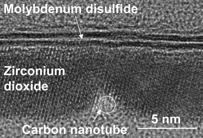
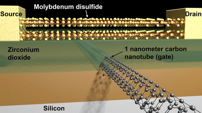
Conventional semiconductor materials will hit a 'brick wall' at 5nm, simply down to the laws of physics, think scientists. However, thanks to the choice of cutting edge materials, the Berkeley Lab team has gained a lot more room for miniaturisation. As described by the Berkeley Lab Blog, the key to the creation of the smallest transistor ever was the use of carbon nanotubes and molybdenum disulfide (MoS2). Carbon nanotubes have been in science and tech news a lot in recent years/months with IBM, for example, describing them as the basis for our 'post-silicon future'. (IBM also saw the potential of combining these carbon structures with molybdenum.)
Berkeley Labs refers to molybdenum disulfide (MoS2), commonly used as an engine lubricant, as its other key material. While electrons travelling through Silicon gates of under 5nm would be "out of control" due to a quantum mechanical phenomenon called tunnelling, the heavier electrons in molybdenum can be controlled with these smaller gate lengths. Furthermore MoS2 can be scaled down to atomically thin sheets, of about 0.65nm thick.


 Reply With Quote


Bookmarks