


http://hexus.net/ce/news/audio-visua...ocessor-specs/
Microsoft has at last revealed details about the holographic processor, central to the HoloLens augmented reality headset's functionality. Earlier in the year Microsoft published specs for the headset ? it explained that the HoloLens was powered by the combination of a 14nm Intel Atom x86 Cherry Trail processor and a 'Microsoft HPU'. Now we have details, including a chip plot, for this HPU.
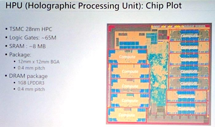
Microsoft devices engineer Nick Baker hosted a presentation at the Hot Chips symposium in California and revealed exactly what is inside Microsoft HPU, reports The Register. The HPU is a custom, TSMC manufactured, 28nm chip which gathers together 24x Tensilica DSP cores. The chip comprises about 65 million logic gates, 8MB of SRAM, and 1GB of LPDDR3 RAM, in a 12mm-by-12mm BGA package. Each of the 24 DSP cores is dedicated to a single sensory I/O computing function.


 Reply With Quote

Bookmarks