


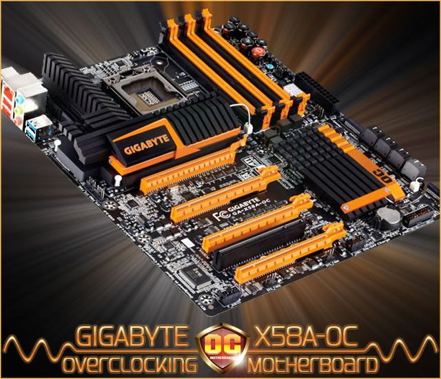
- Gigabyte GA-X58A-OC Review -
- Featuring 4.8-5GHz Testing Vs. UD7 & 9182 - 6GB/s -
Today we will be looking at the GA-X58A-OC motherboard, GIGABYTE's new ground breaking entry in the 1366 motherboard lineup. While the X58 chipset isn't new, and there are other newer alternative chipsets, X58 is still the top-tier chipset of Intel's motherboard platform offerings. Intel has recently released a few new CPU's for the 1366 socket boards as well, the i7-990X and i7-980, and these processors (along with older models) and motherboards are still delivering record breaking results and offering massive performance for the end user.
During CES 2011 this past January, GIGABYTE briefly (about 5 seconds) showed an image of an upcoming mystery orange and black motherboard. Since then, the buzz around the internet about this board has steadily increased, and as time passed Hicookie began to break benchmarking records and release various videos and images of the board in action. A month or two later Colin (Technical Marketing Manager) and Hicookie made a few rounds doing interviews where they spoke in more detail about the board, offering the public a more detailed look at the board, and gave a multitude of information on the design & planning stages telling us how this motherboard came to life. They also talked in depth about what features were added or removed, and why, and mentioned a very reasonable entry price point, giving overclockers even more to dream about.
As with any product discussed early in the design and production phase, nothing is ever as easy as it seems, and due to some features of the board having to be redesigned, and the Intel P67 B2 chipset recall, board production was delayed, and the eventual release price was a fair amount more than initially expected. Finally, on May 5, 2011, the GA-X58A-OC motherboard started shipping to retailers worldwide from the Gigabyte factory in Taiwan. Since that time, and before, it has been breaking motherboard benchmarking records around every corner.
The X58A-OC is designed drastically different in comparison to other motherboards in GIGABYTE's lineup, and it's notably different than any other motherboards from any manufacturer. The X58A-OC's main purpose and intended use is to push the boundaries of motherboard design into a direction suitable for extreme overclocking. There have been other motherboards created for overclockers in the past, by various brands including GIGABYTE, however, the board under review today has had many features removed in comparison to other previous motherboards, and has multiple newly added features with the sole intent being to deliver the board into the hands of extreme overclockers using liquid nitrogen or dry ice cooling. The X58A-OC motherboard was born from a dream of GIGABYTE's in-house benchmarking champion and engineer Hicookie. Hicookie worked closely with GIGABYTE's various in-house departments, and jokingly mentioned that at times this was not an easy task - laughing about various aspects of his intended design which the various departments could never agree upon. In the end they were able to decide what would finally be included on the board and what could be removed. Once everything was finalized, a monstrous motherboard was welcomed into existence, able to deliver record breaking results, while at the same time becoming more ideal for the work/play of extreme overclockers.
Many of the normal motherboard features such as 10+ USB ports, Dual LAN, eSATA, IDE ect. to name a few, have been removed in order to allow for those expenses to be used in other areas of design. After removing many of the various features from a motherboard that extreme overclockers do not utilize, or that they disable from the very first entry into the BIOS, this left the board with a minimal set of features that overclockers would use, and a few that the Marketing team decided were a must (Audio, 4G button, SATA 6Gb/s, USB3). This left a decent amount of allocated resources that could be used for other exciting features that an extreme overclocker desires, such as multiple on-board temperature sensors, easier to insulate components (POSCAP capacitors across the entire board), on-board voltage readout points, PWM frequency dip-switch, Dual BIOS dip-switch allowing the user to choose which BIOS chip to boot from, and GIGABYTE's new "Gear" and +/- frequency and ratio buttons. These removals and deviations from the normal design path also allowed them to keep the board's final cost to a minimal amount, while still allowing the addition of these new features and high end components.
Here's some quick information about GIGABYTE before we get started on the review.
Originally Posted by GIGABYTE
Introducing the Gigabyte GA-X58A-OC motherboard
Gigabyte's full specifications for the GA-X58A-OC, and the product overview which some of the following will cover, can be found here:
GIGABYTE GA-X58A-OC Motherboard Overview
Unique Features:
GA-X58A-OC Technical Specifications:
CPU
1. Support for an Intel® Core i7 series processor in the LGA1366 package
2. L3 cache varies with CPU
QPI
1. 4.8GT/s, 6.4GT/s
Chipset
1. North Bridge: Intel® X58 Express Chipset
2. South Bridge: Intel® ICH10R
Memory
1. 6 x 1.5V DDR3 DIMM sockets supporting up to 24 GB of system memory
2. 3/Dual channel memory architecture
3. Support for DDR3 2200/1333/1066/800 MHz memory modules
4. Support for non-ECC memory modules
5. Support for Extreme Memory Profile (XMP) memory modules
Audio
1. Realtek ALC889 codec
2. High Definition Audio
3. 2/4/5.1/7.1-channel
4. Support for S/PDIF Out
LAN
1. 1 x Realtek RTL8111E chip (10/100/1000 Mbit)
Expansion Slots
1. 2 x PCI Express x16 slots, running at x16 (PCIEX16_1, PCIEX16_2)
2. 2 x PCI Express x16 slots, running at x8 (PCIEX8_1, PCIEX8_2)
3. 1 x PCI slot
Multi-Graphics Technology
1. Support for 3-Way/2-Way NVIDIA SLI technology and 4-Way/3-Way/2-Way ATI CrossFireX technology
Storage Interface
South Bridge:
1. 6 x SATA 3Gb/s connectors (SATA2_0~SATA2_5) supporting up to 6 SATA 3Gb/s devices
2. Support for SATA RAID 0, RAID 1, RAID 5, and RAID 10
1 x Marvell 88SE9182 chip:
1. 2 x SATA 6Gb/s connectors (GSATA3_6, GSATA3_7) supporting up to 2 SATA 6Gb/s devices
2. Support for SATA RAID 0 and RAID 1
USB
South Bridge:
1. Up to 4 USB 2.0/1.1 ports (2 on the back panel, 2 via the USB bracket connected to the internal USB header)
1 x Etron EJ168 chip:
1. Up to 2 USB 3.0/2.0 ports on the back panel
Internal I/O Connectors
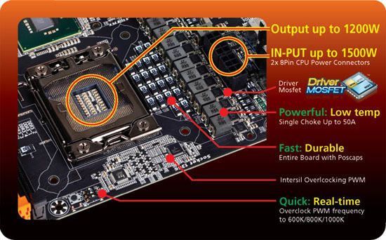
1. 1 x 24-pin ATX main power connector
2. 2 x 8-pin ATX 12V power connectors
3. 2 x PCIe power connectors
4. 2 x SATA 6Gb/s connectors
5. 6 x SATA 3Gb/s connectors
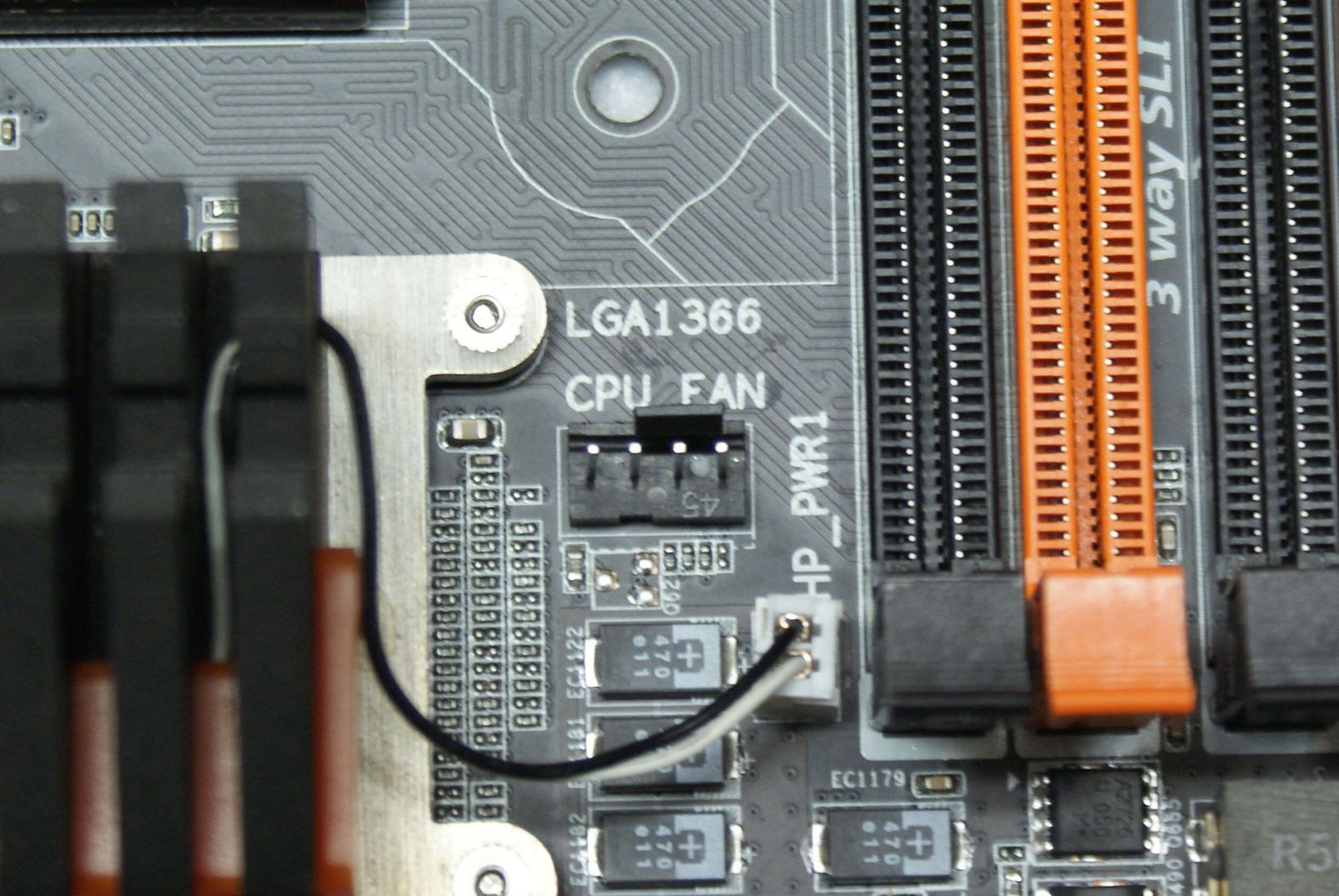
6. 1 x CPU fan header
7. 6 x system fan headers
8. 1 x North Bridge fan header
9. 1 x front panel header
10. 1 x front panel audio header
11. 1 x S/PDIF Out header
12. 1 x USB 2.0/1.1 header
13. 2 x heatsink LED power connectors
14. 1 x clearing CMOS button
15. 1 x power button
16. 1 x reset button
17. 1 x PWM frequency switch
18. 1 x onboard voltage measurement module
19. 1 x 4G Ready button
20. 1 x OC Gear button
21. 1 x CPU BCLK Down button
22. 1 x CPU BCLK Up button
23. 1 x CPU Ratio Down button
24. 1 x CPU Ratio Up button
25. 1 x BIOS switch
Back Panel Connectors
1. 1 x PS/2 keyboard port
2. 1 x PS/2 mouse port
3. 2 x USB 2.0/1.1 ports
4. 2 x USB 3.0/2.0 ports
5. 1 x RJ-45 port
6. 3 x audio jacks (Line In/Mic In/Line Out)
I/O Controller
1. iTE IT8720 chip
H/W Monitoring
1. System voltage detection
2. CPU/System temperature detection
3. CPU/System fan speed detection
4. CPU overheating warning
5. CPU/System fan fail warning
6. CPU/System fan speed control
BIOS
1. 2 x 16 Mbit flash
2. Use of licensed AWARD BIOS
3. Support for DualBIOS
4. PnP 1.0a, DMI 2.0, SM BIOS 2.4, ACPI 1.0b
Unique Features
1. Support for @BIOS
2. Support for Q-Flash
3. Support for Xpress BIOS Rescue
4. Support for Download Center
5. Support for Xpress Install
6. Support for Xpress Recovery2
7. Support for EasyTune
8. Support for Smart 6
9. Support for Auto Green
10. Support for eXtreme Hard Drive (X.H.D)
11. Support for ON/OFF Charge
12. Support for Cloud OC
13. Support for Q-Share
Form Factor
1. ATX Form Factor; 30.5cm x 26.4cm
Product Images:
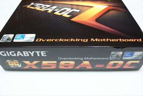
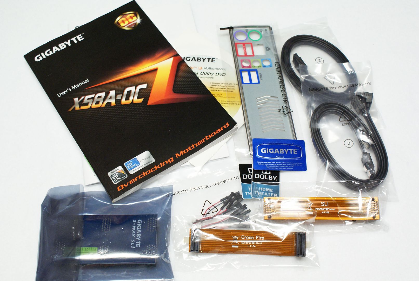
Packaging & Included Accessories:

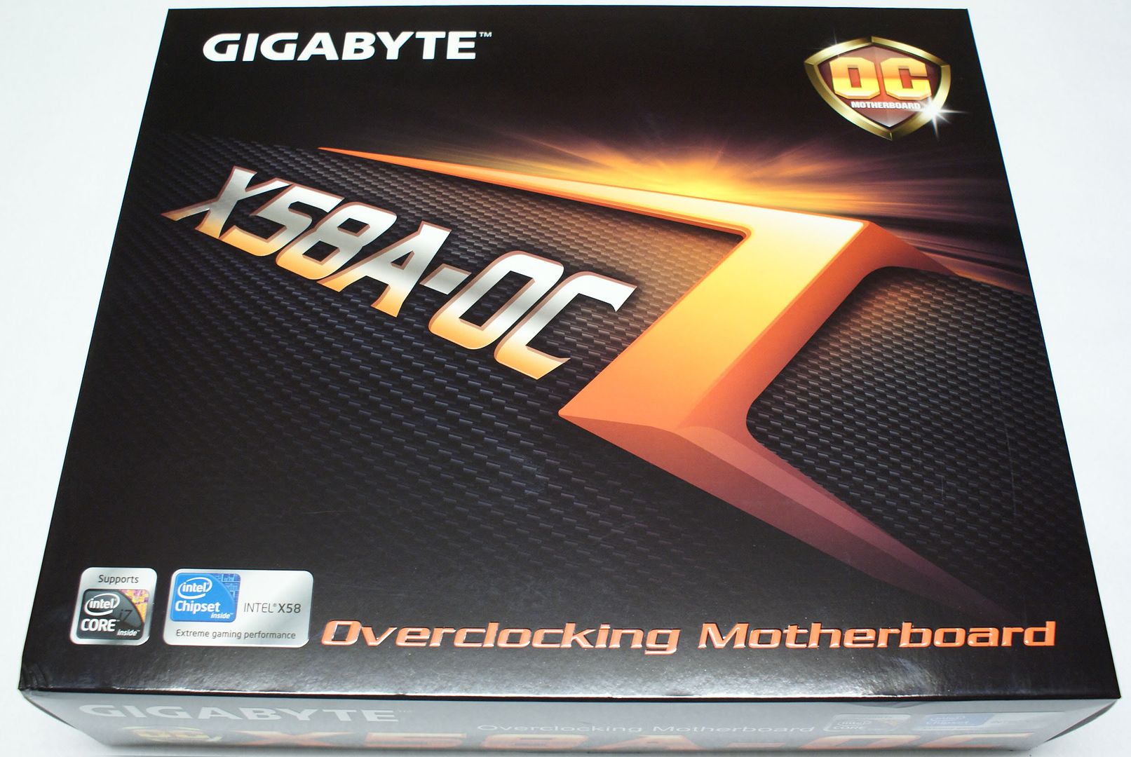
Here we can see the X58A-OC packaging, with the outer box done in black with hints of orange on much of the text. On the front of the box is the "OC" logo and model name along with a three-dimensional neon orange graphic and a few Intel badges. On the rear of the box the board itself is shown centered, with the new "OC" features inscribed in detail surrounding it.
On the sides of the box we see the usual items, Intel badges, motherboard model and brand names, along with a 3-point features and benefits section in several languages.
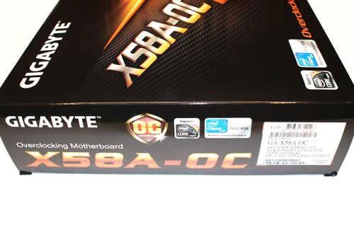
This is the opposite side, showing the same emblems and the model name, this side also has the box label that includes the board revision, serial number, short list of specs and the product UPC Code. Next we have the inner package that actually contains the motherboard itself, GIGABYTE chose to use a plain cardboard box for this as it cuts down on packaging costs allowing more funds to be spent on the board itself. This is perfectly fine as the inner box is rarely seen or used, and it safely and securely holds the motherboard.
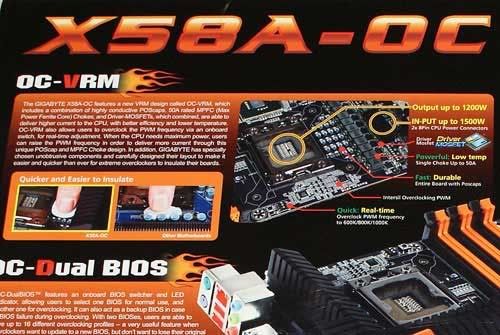
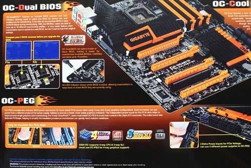
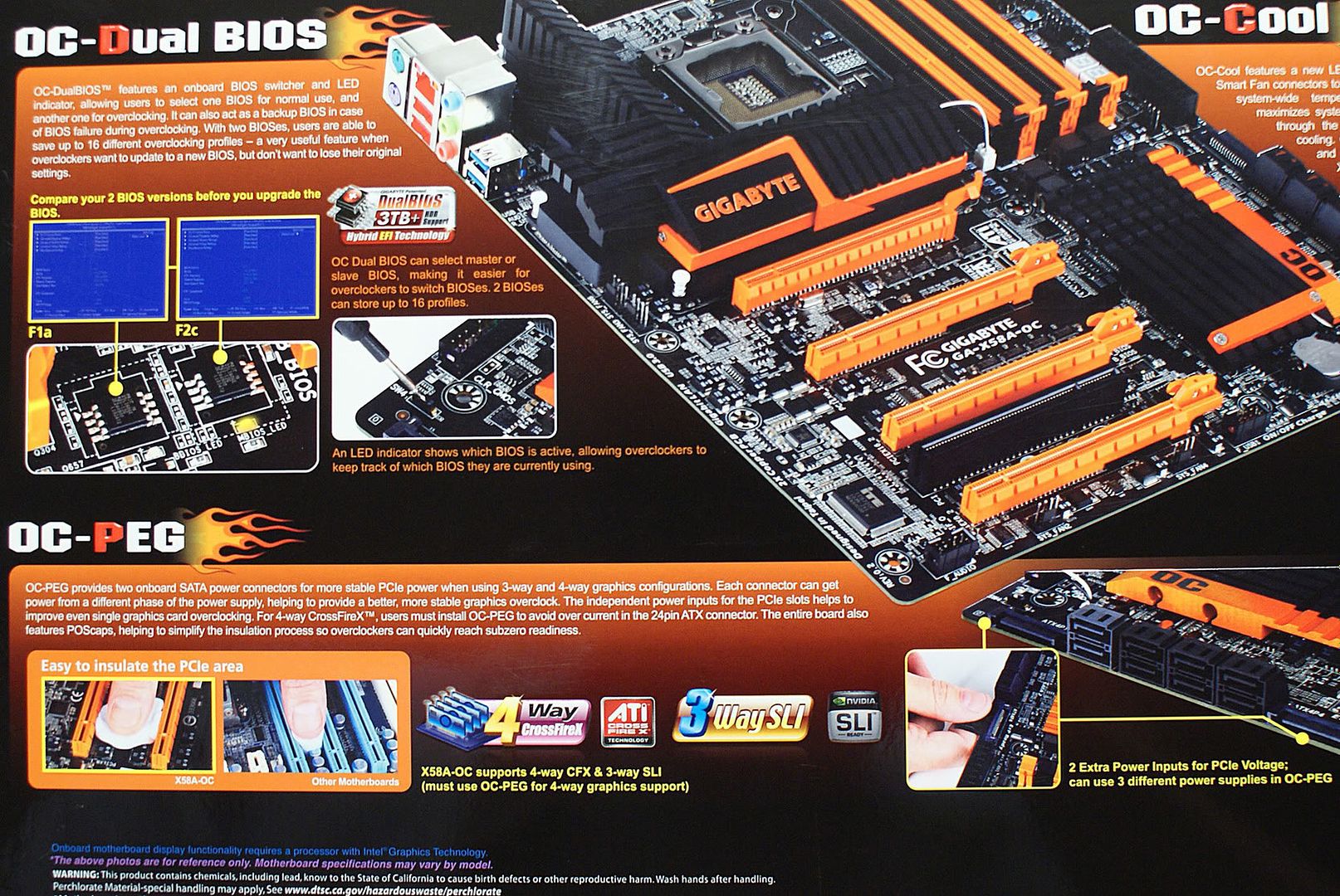
Up-close shots of the back of the box show more detail about all of the new "OC" features. These would be OC- VRM, OC-Touch, OC-Dual BIOS, OC-PEG, and OC-Cool. These are all very noteworthy new features, and GIGABYTE has outlined them very well on the package itself (Same as shown above in Unique Features section).
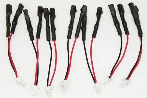
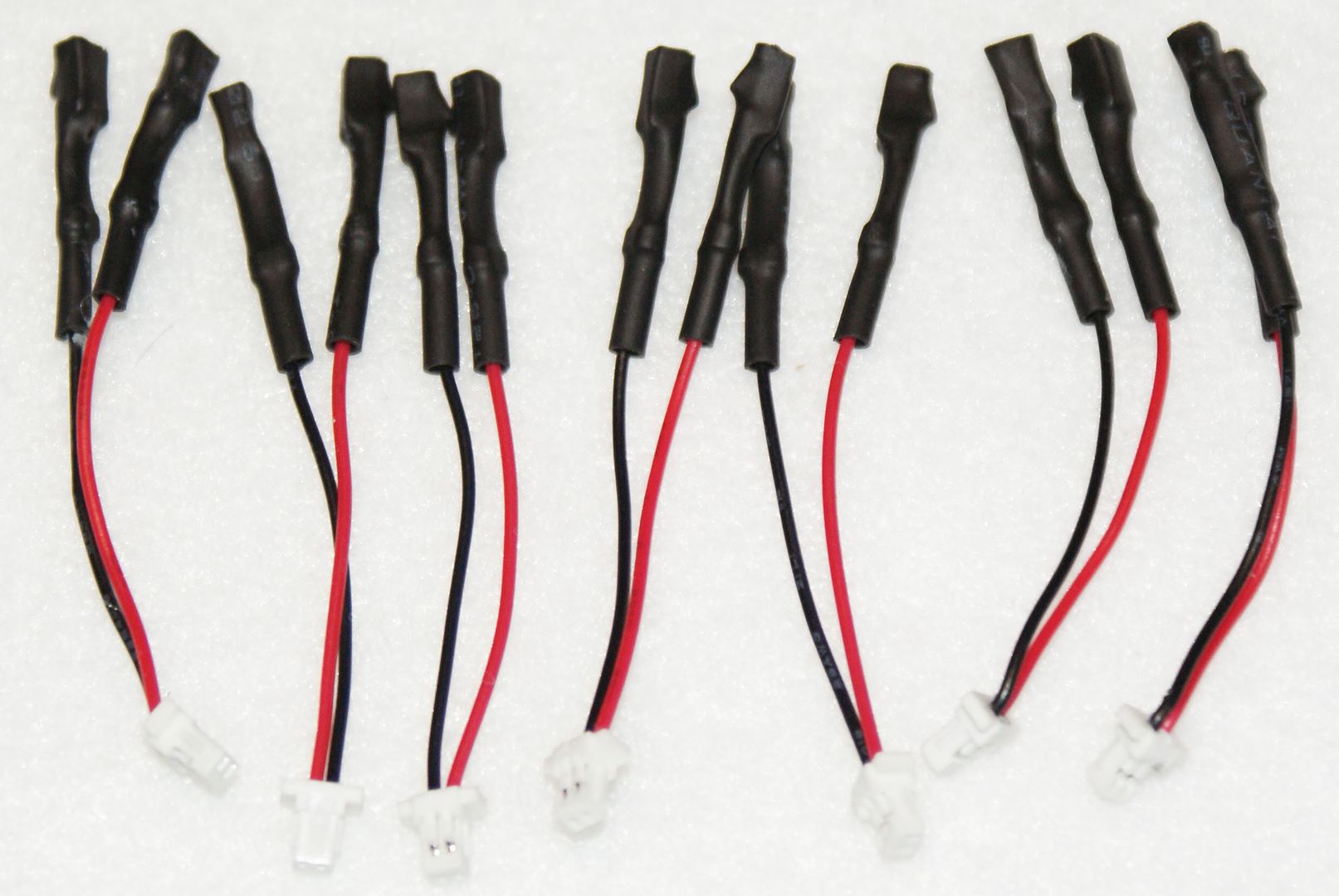
These are the included voltage readout cables which attach directly to headers on the motherboard near the power button. Most any DMM (Digital Multi-Meter) will fit into these cables, and GIGABYTE has included 7 of them, one for each voltage readout point on the board.
Here are all of the included accessories, specifically the installation guides, and motherboard manual and driver CD, 4 Black SATA Cables, Vented I/O shield, Dual SLI and Crossfire cables, SLI 3-way PCB Connector, 7 voltage readout cables, and Dolby and Gigabyte case badge stickers.
Motherboard Itself:
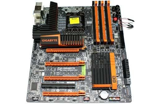
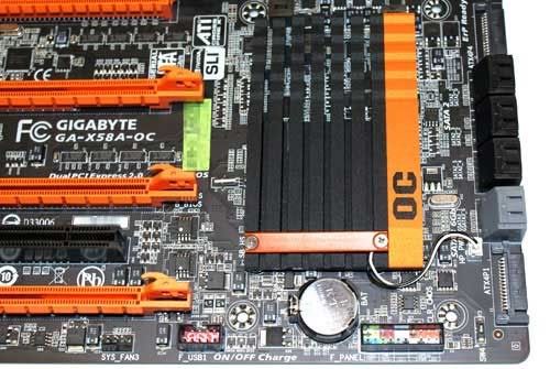
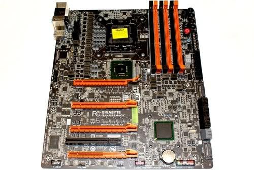
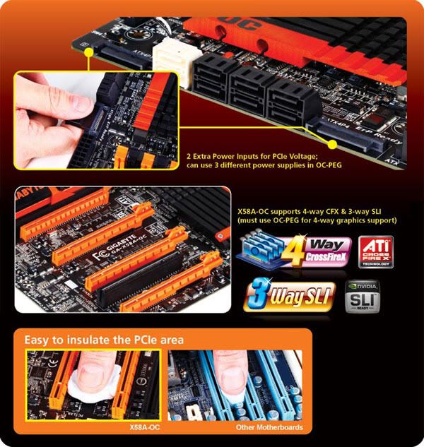
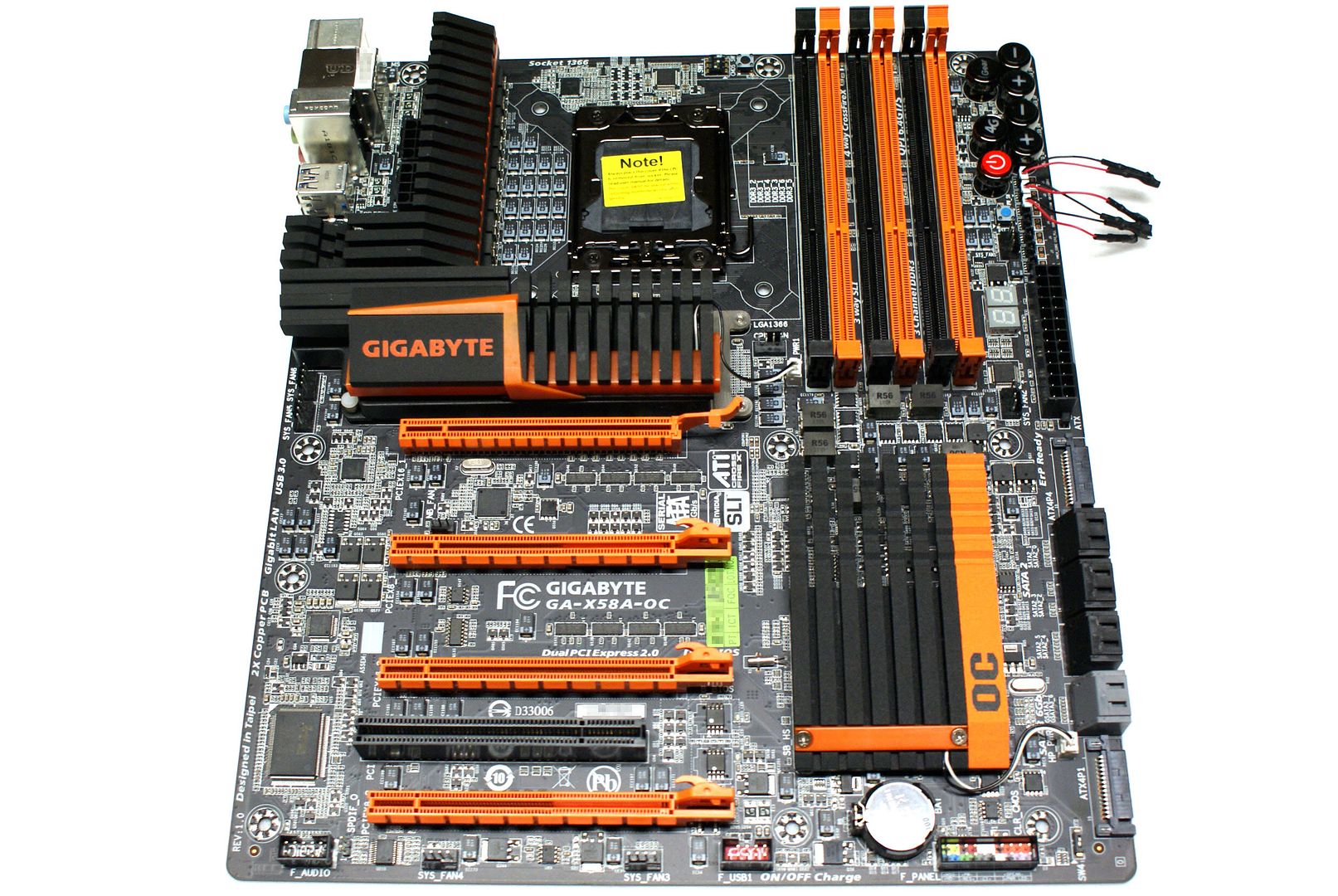
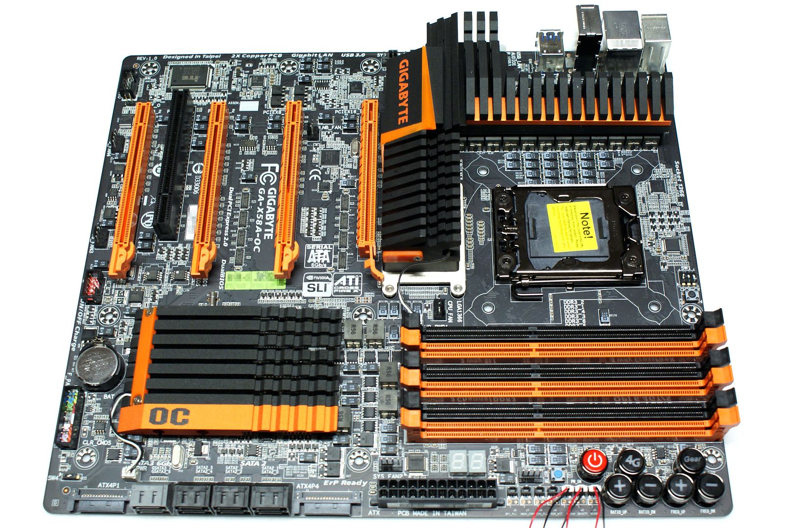
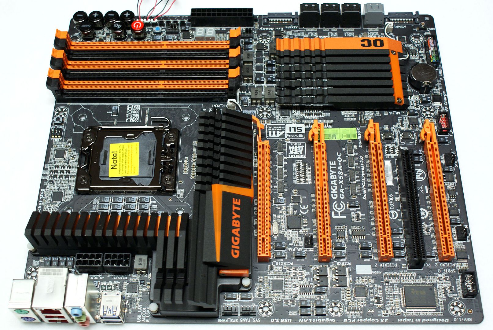
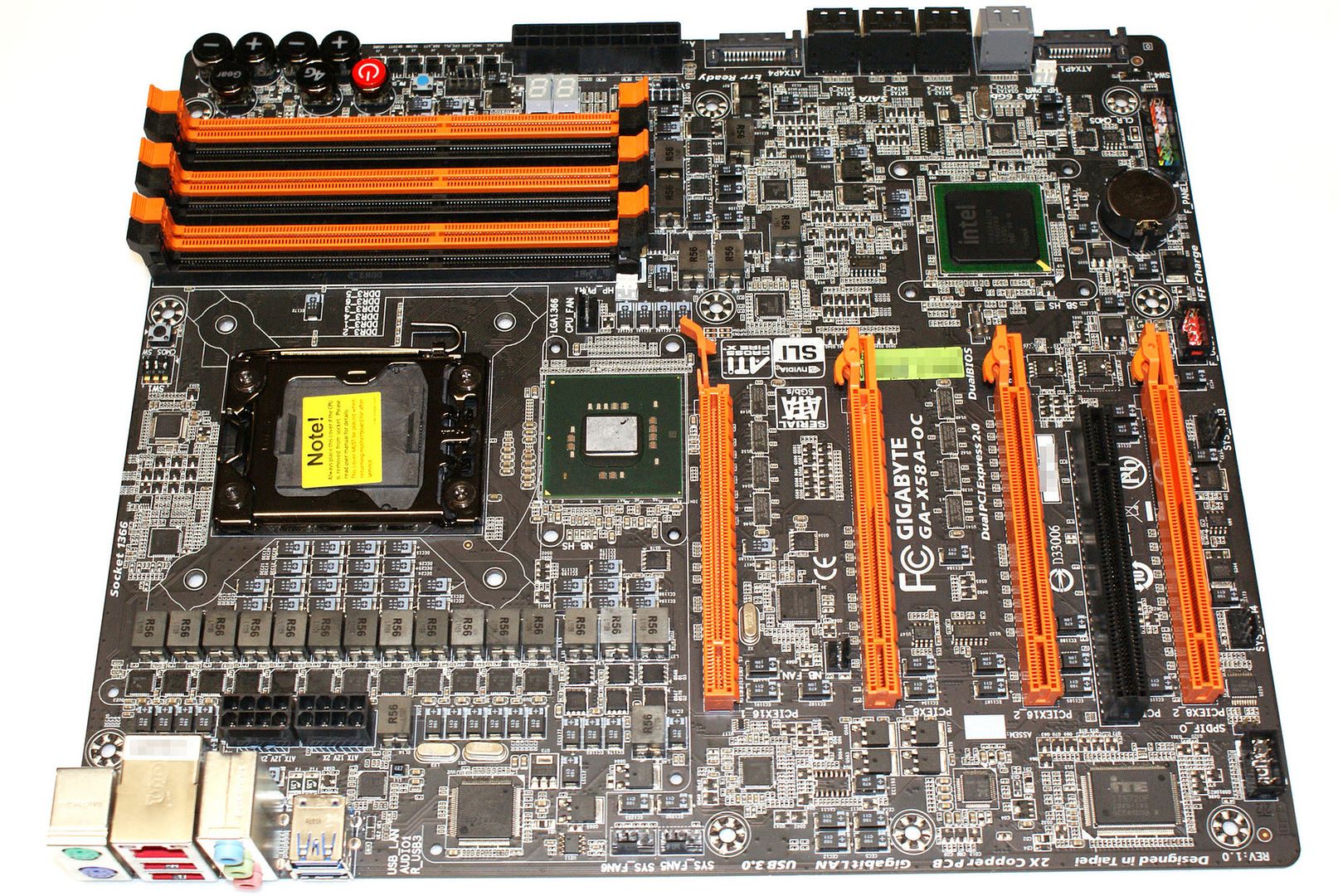
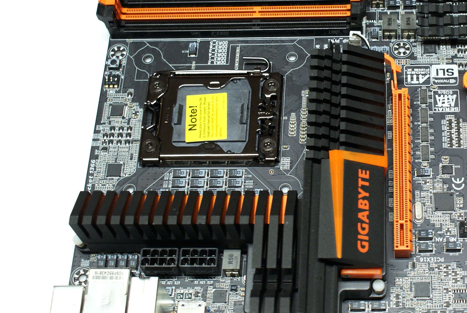
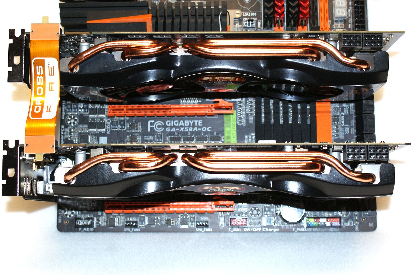
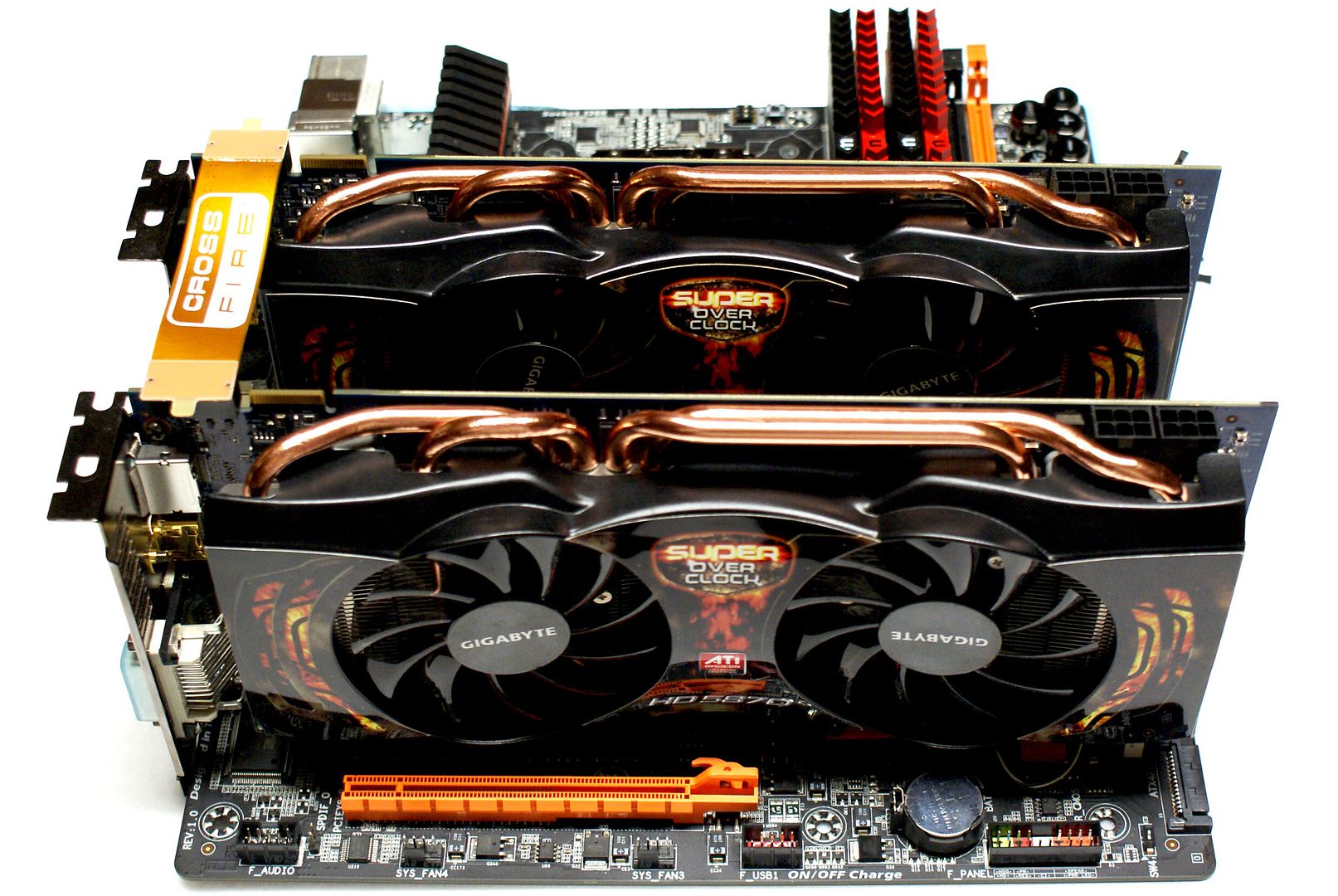
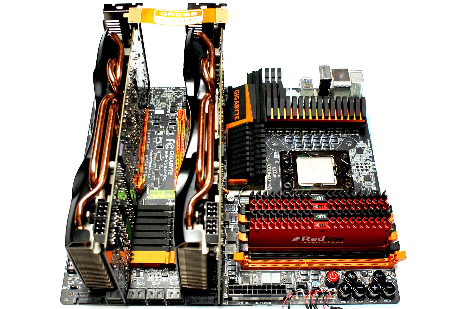
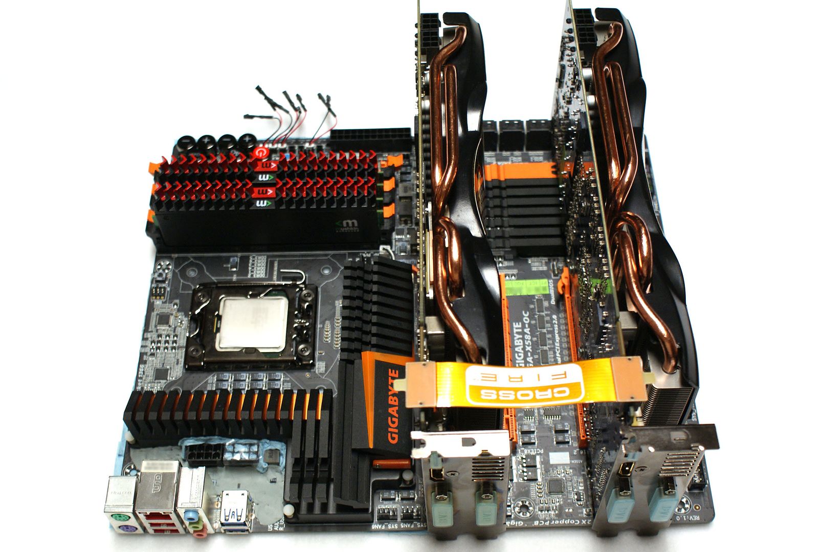
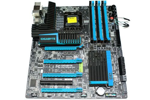
As you can see, the board itself is done with GIGABYTE's new (Real) Black PCB, and accented in a bright orange. The PCIE spacing is set wide, leaving plenty of room for larger cards (I'll show this in more detail further in the review). The GA-X58A-OC provides 32 PCI Express lanes for graphics, those are split into dual PCIE x16 slots, and two PCI Express x8 ports. You can run two-way Crossfire or SLI at x16/x16, or three-way at x16/x8/x8, and Crossfire with four cards can also be utilized at x8/x8/x8/x8 (ATI Only).
You can see this board includes many features just from a quick glance, the new on-board buttons and switches are easily visible. You can also see that this board offers some unique features that GIGABYTE has not used in the past, such as voltage read points, and SATA power attachments directly on the board (OC-PEG).

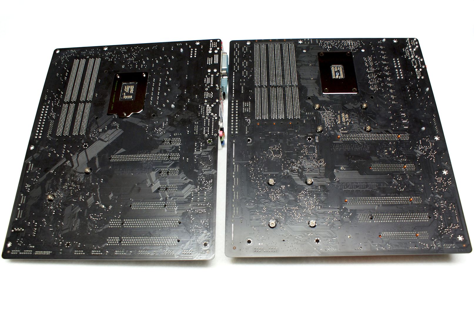
Here you can get a closer look at the NB (IOH) heatsink, and see that this board offers dual ATX 12V connections for attaching two power supplies to deliver maximum power. We can also see that this is a 6 layer PCB, in contrast to the UD7's 8 layers, for example. This is likely a cost-cutting measure in order to deliver higher quality components to other areas of the board. The board still carries GIGABYTE's traditional Ultra Durable 3 design with 2oz copper PCB offering better cooling capabilities and better electrical delivery.
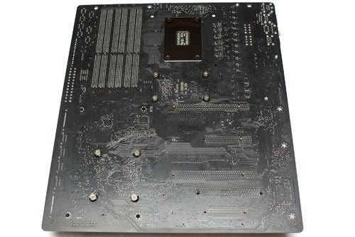
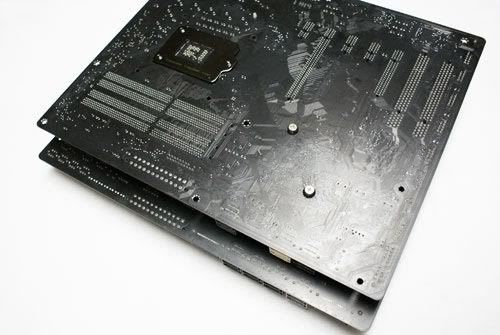
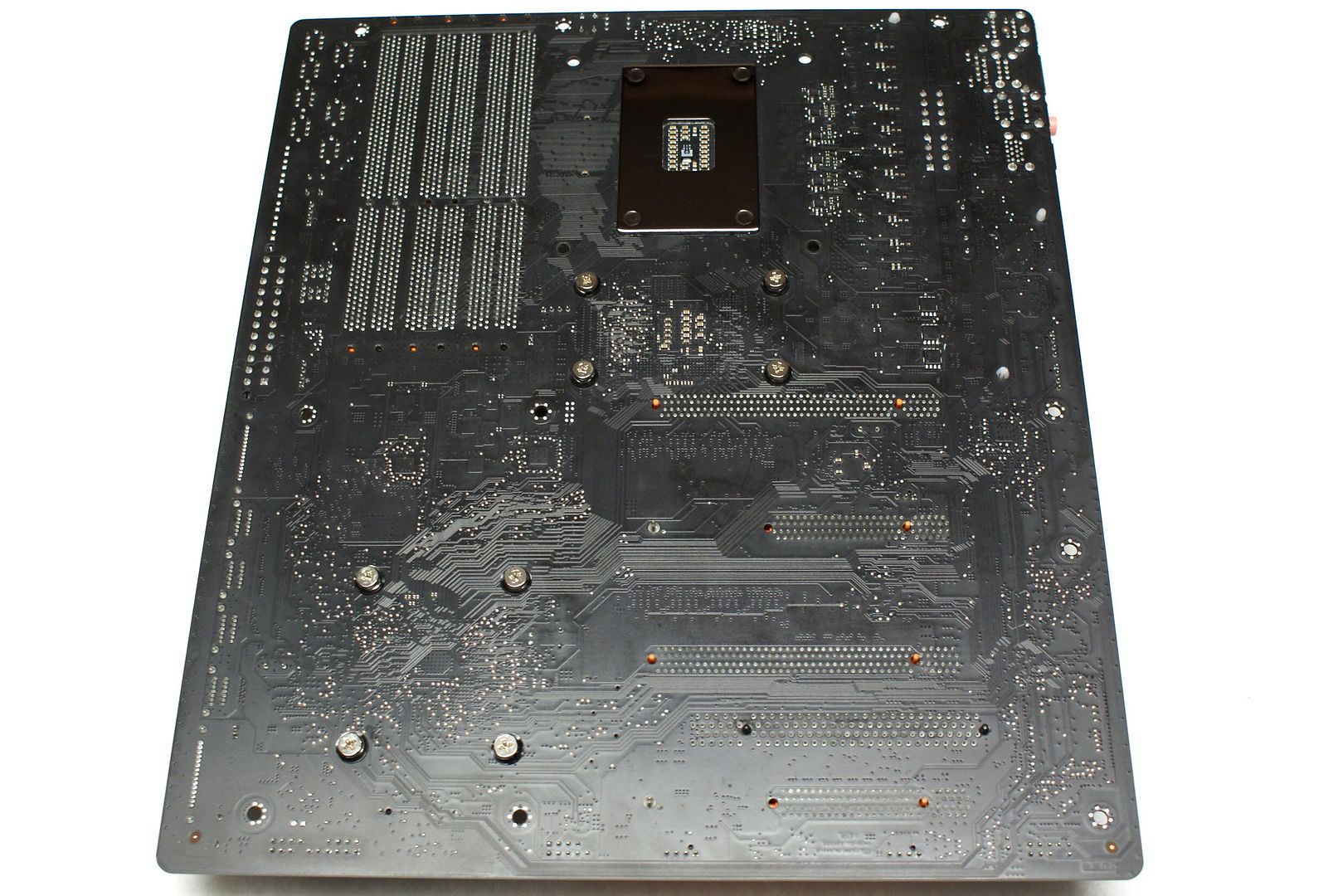
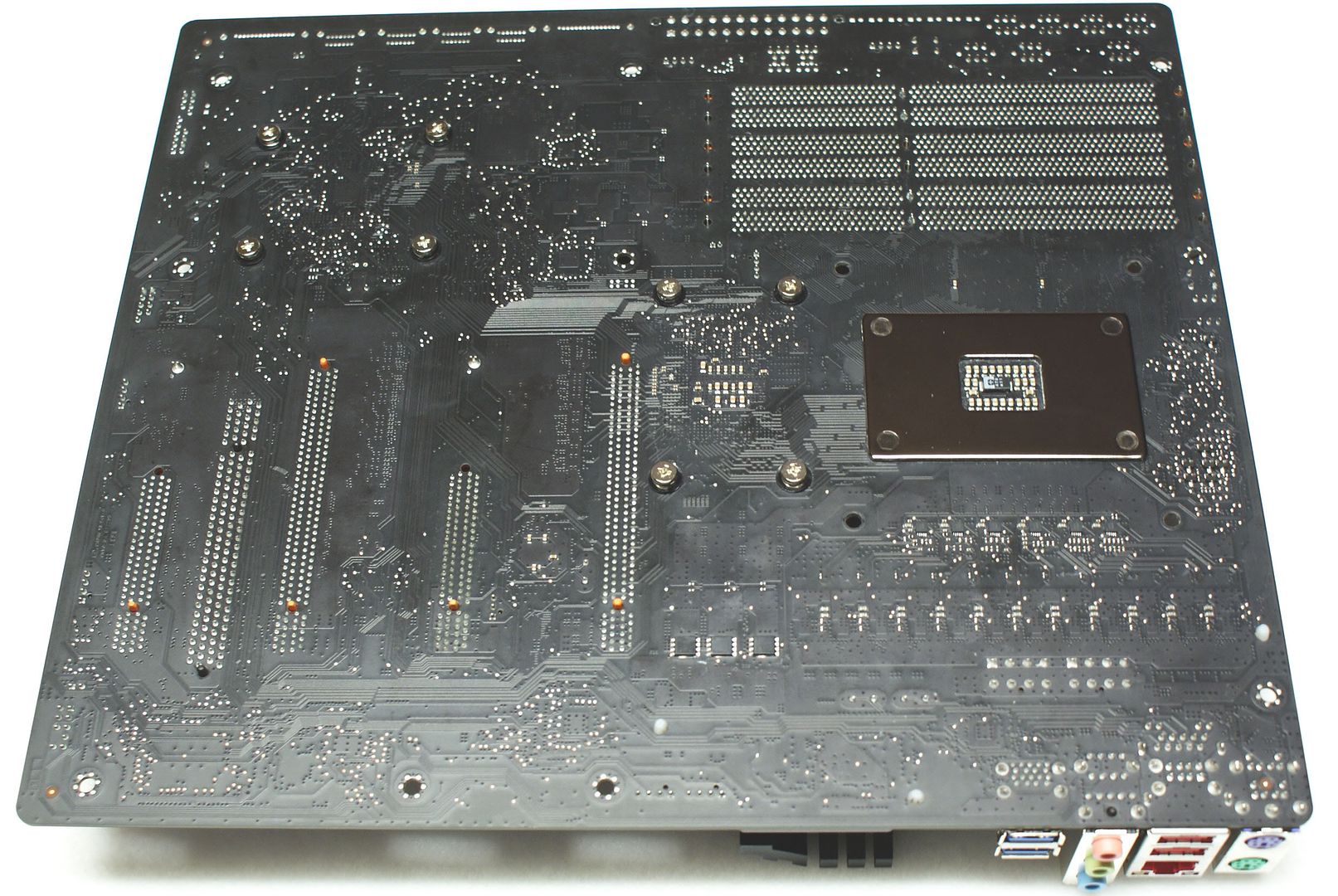
On the reverse we can see that the north and south bridge heatsinks are secured in place with screws instead of push-pins used on lesser budget oriented boards, however, the VRM part of the heatsink is held in place with push-pins. You can also see just how dark GIGABYTE's new black PCB is, it's actually a very solid black, instead of see-through black with unattractive copper traces showing through.
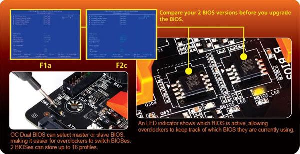
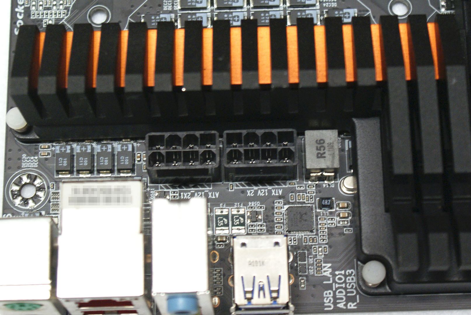
Here is an up-close shot of the Dual ATX 12V connections, better get your power supplies ready! You can also see part of the OC-Dual BIOS here, this is the Main and Backup BIOS chips, along with an LED for each one which lights up when powered on to indicate which BIOS is in use.
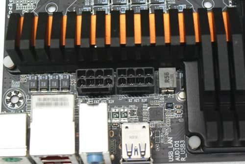
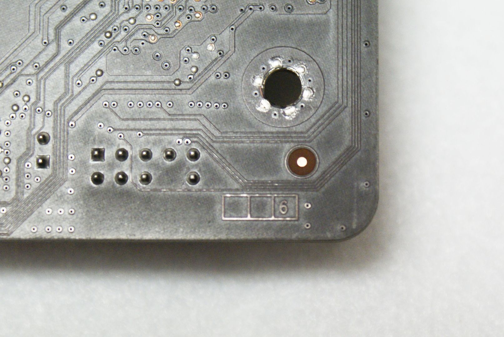
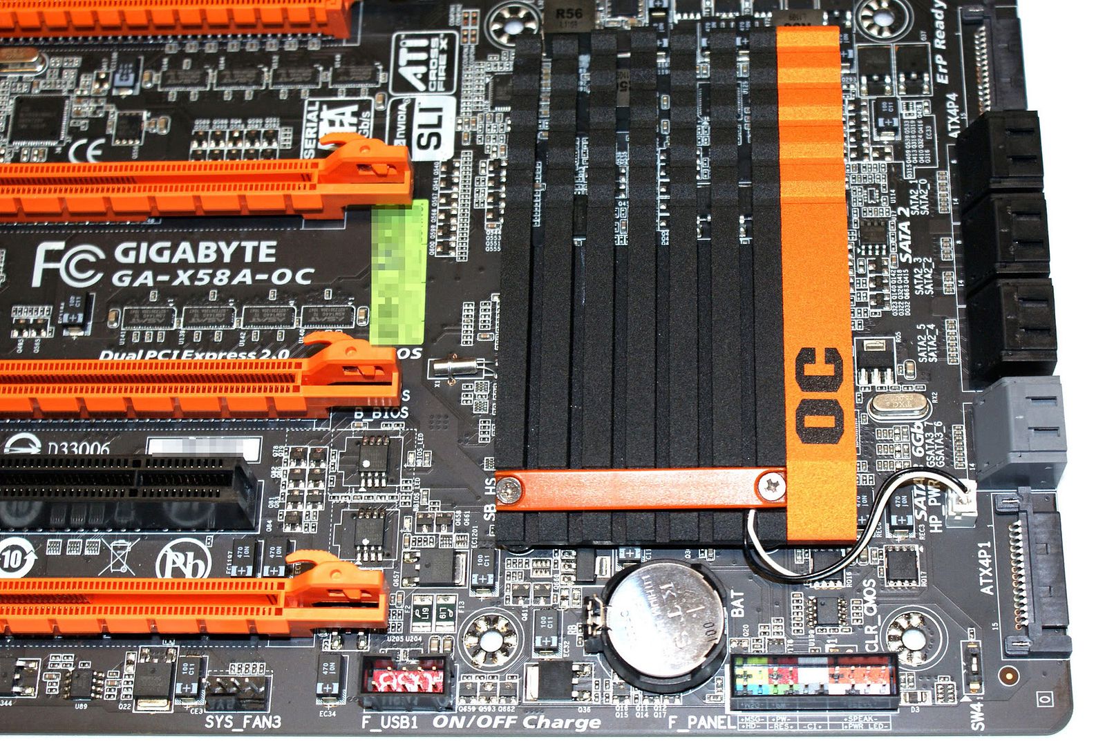
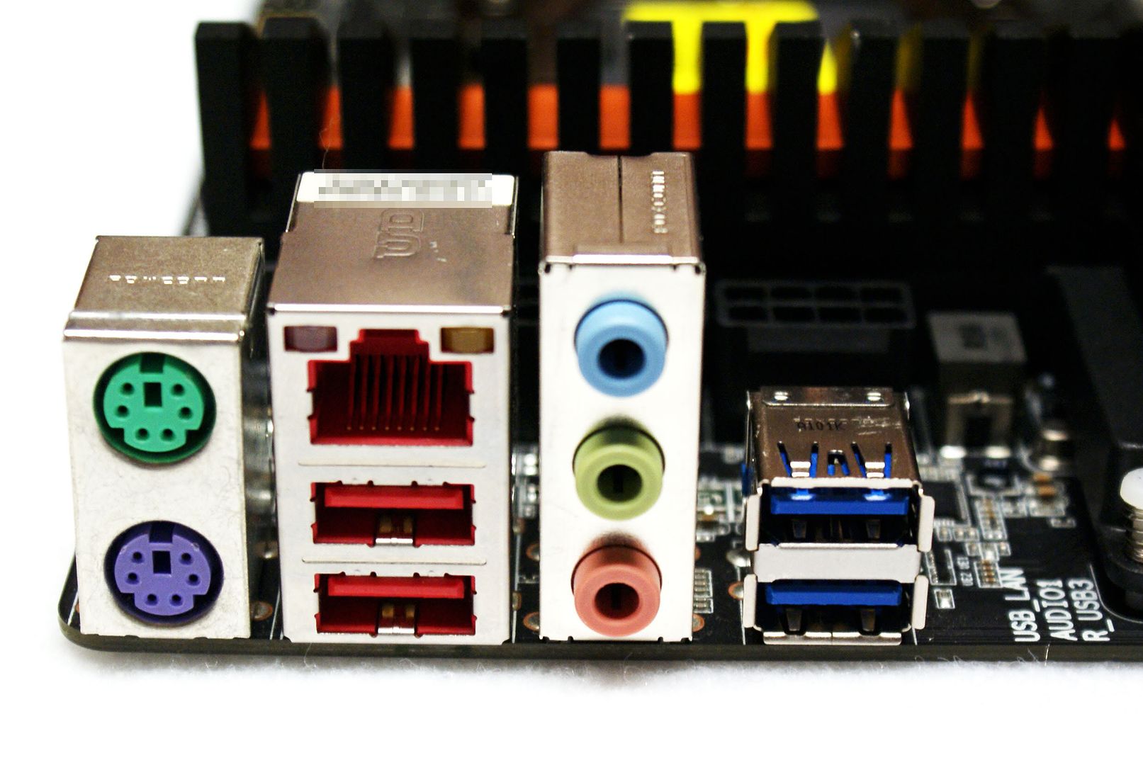
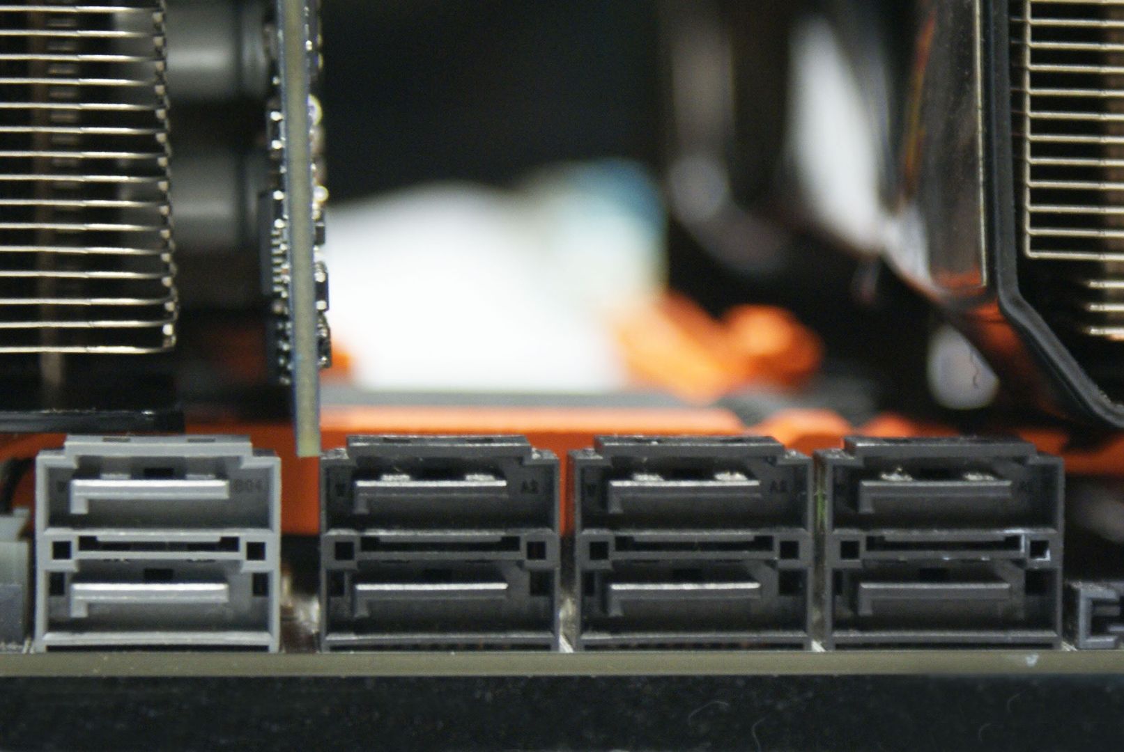
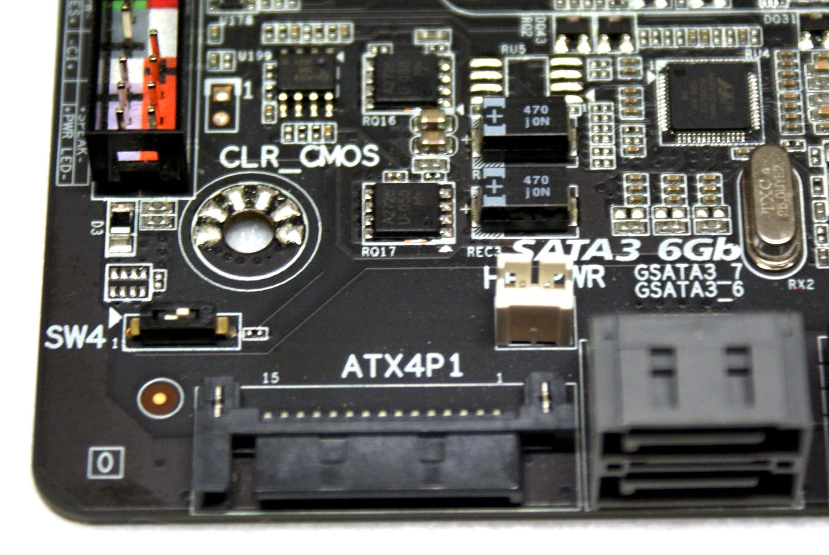
Here is a close-up shot of the lower SB corner of the board, the wire coming from the SB heatsink powers a set of orange LEDs, there is a set of LEDs in the NB as well. You can see this board has USB On/Off charge to charge your iPhone or other USB devices directly from the motherboard whether it is on or off. We also see here the front panel header, 8 SATA ports (2 of which are 6Gb/s), and the OC-PEG SATA power connections. On the I/O side of things we have the Realtek audio connections, Gigabit Ethernet port, 2 USB3 ports, and a PS/2 mouse and keyboard port.
Here is a comparison of the X58A-OC's Enhanced ATX (EATX) size 30.5cm x 26.4cm, compared to a normal sized ATX Z68X-UD3H motherboard (which I'll have a review out on shortly) coming in at 30.5cm x 24.4cm. The EATX is 2CM wider, but the mounting holes are in the same places so the X58A-OC should fit in most average sized ATX cases. You may run into some issues though if you try to squeeze this board into a small form factor ATX Case, so be sure you check measurements if you're thinking of using a smaller case.
Motherboard - Heatsinks Removed:
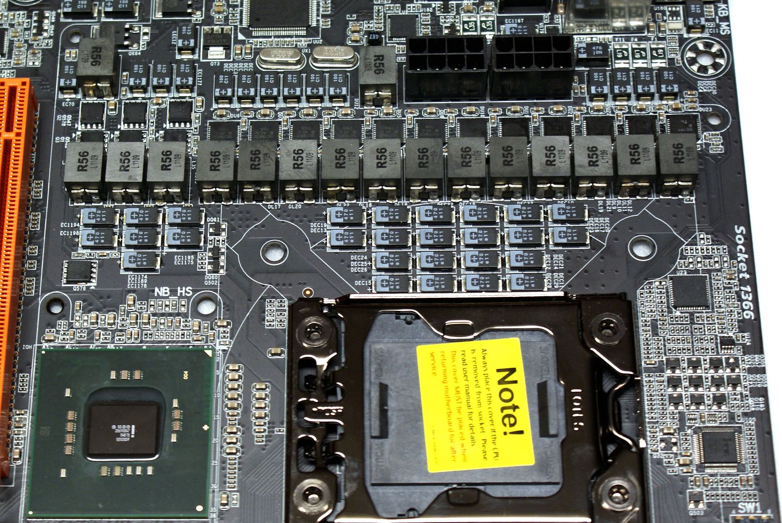
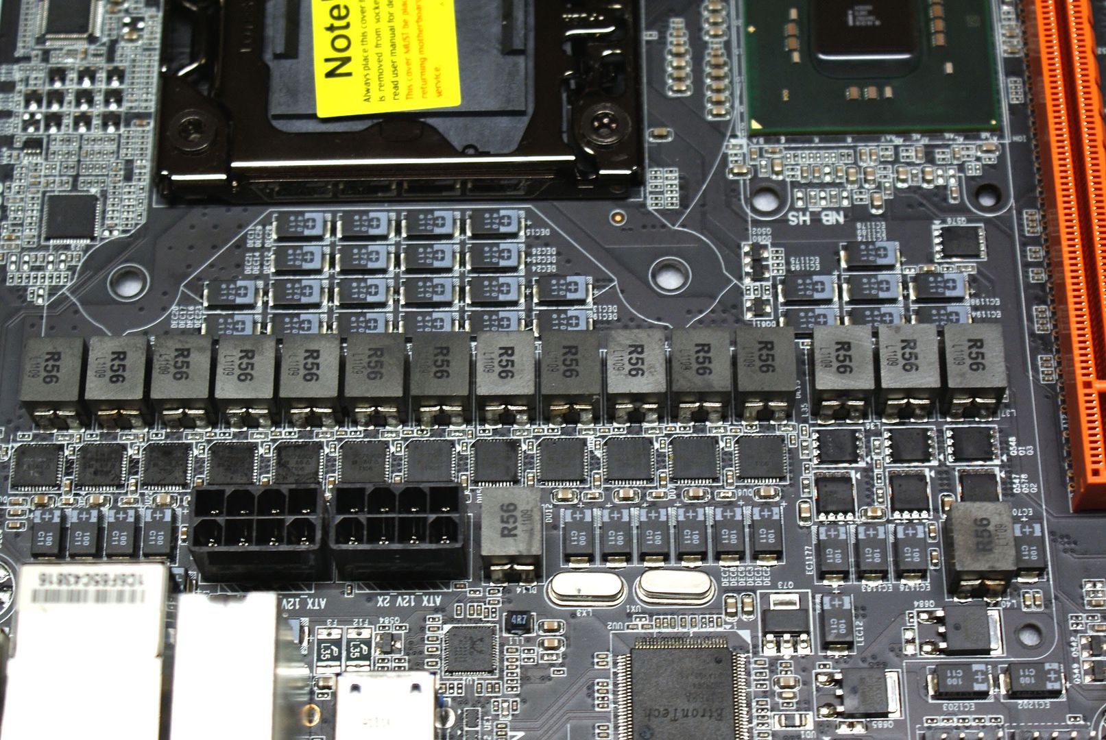
Here is the board naked, with all heatsinks removed. You can see the 12-phase 'dual power' processor voltage regulation module (VRM), it's designed to deliver up to 600A output to the CPU. The other phases are for the Uncore, which is a a 4-phase design, and there is an additional 3 phases for the memory and 3 phases for the IOH as well. POSCAP tantalum capacitors (Surface mount) are used across the board, they are more reliable, easier to insulate around, and they save space. There is not even a single barrel or can-type older solid capacitor on this motherboard, it's all POSCAP!
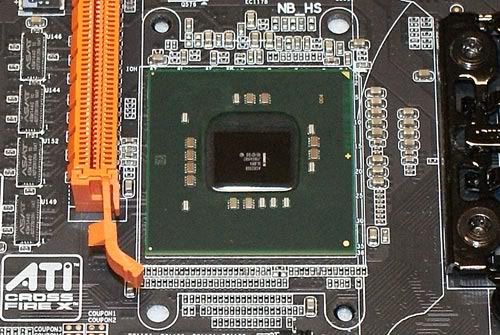
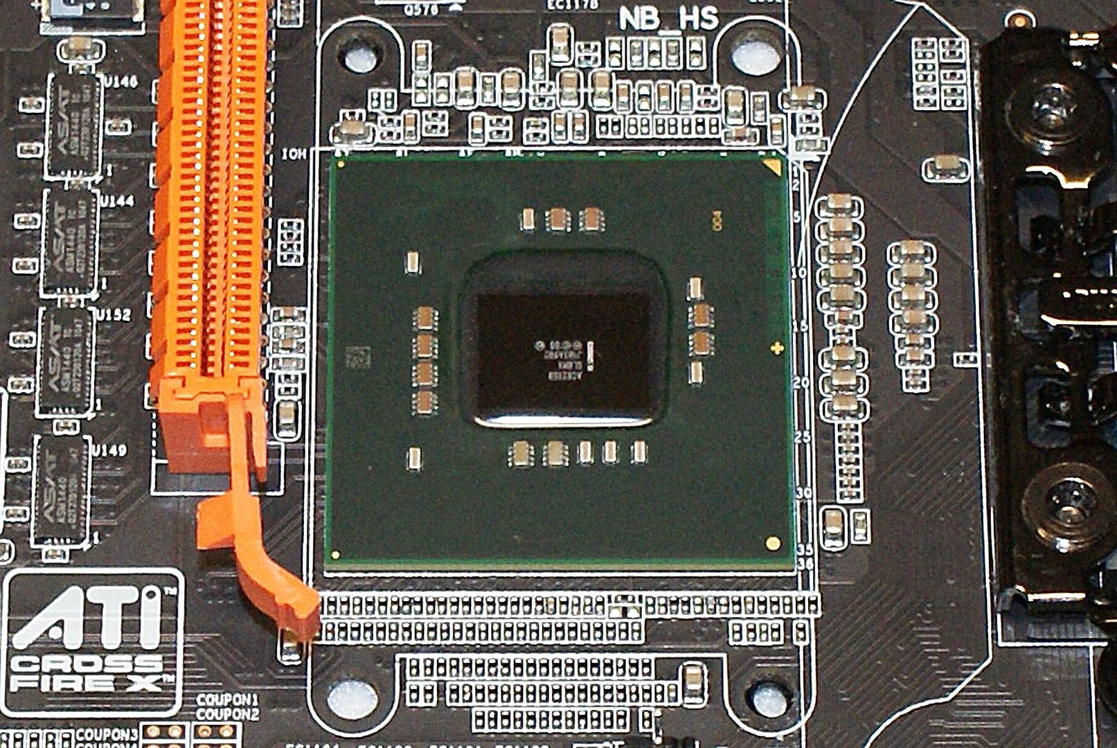
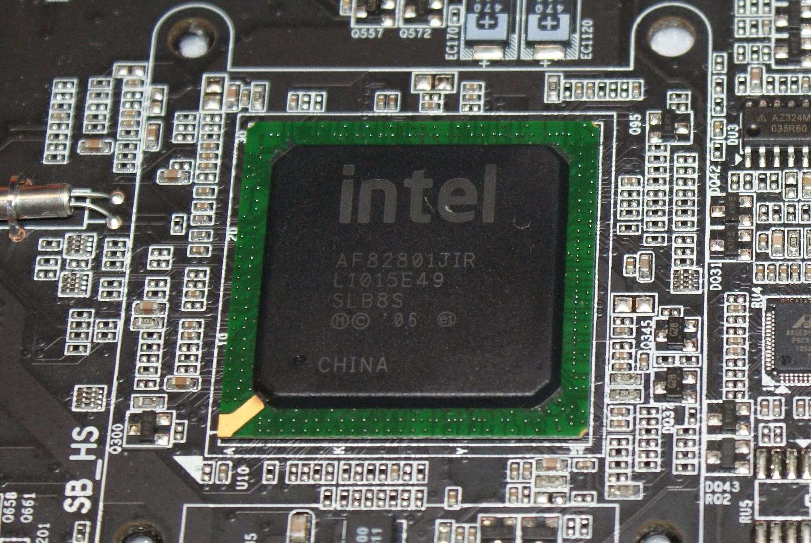
Here is a close-up of the NB (MCH) X58 chipset, and the ICH10R SB chipset. Click any image in this review for a much larger look!
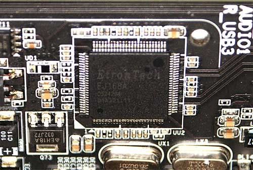
Here we can see the newly certified Etron EJ168A USB 3.0 controller, this controls the USB 3.0/2.0 ports on the rear of the motherboard. Also shown is the new and impressive Marvell SE9182 SATA 6Gb/s controller. This should not be confused with the older Marvell 9128 controller, the new 9182 controller has it's own actual BIOS (Hardware level RAID), and utilizes dual PCIE x1 lanes for double the bandwidth of the previous 9128 controller that was limited by a single PCIE x1 lane. This controller also offers RAID Stripe sizes up to 128k vs. the 9128's 64k upper limit.

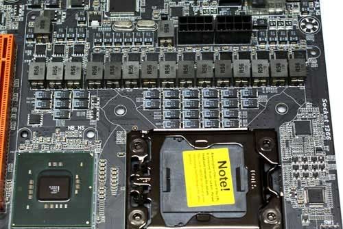
Here is a much closer look at GIGABYTE's new VRM layout for the OC power delivery, in these images you can see the 12 VRM phases for the CPU, and 4 for the Uncore.
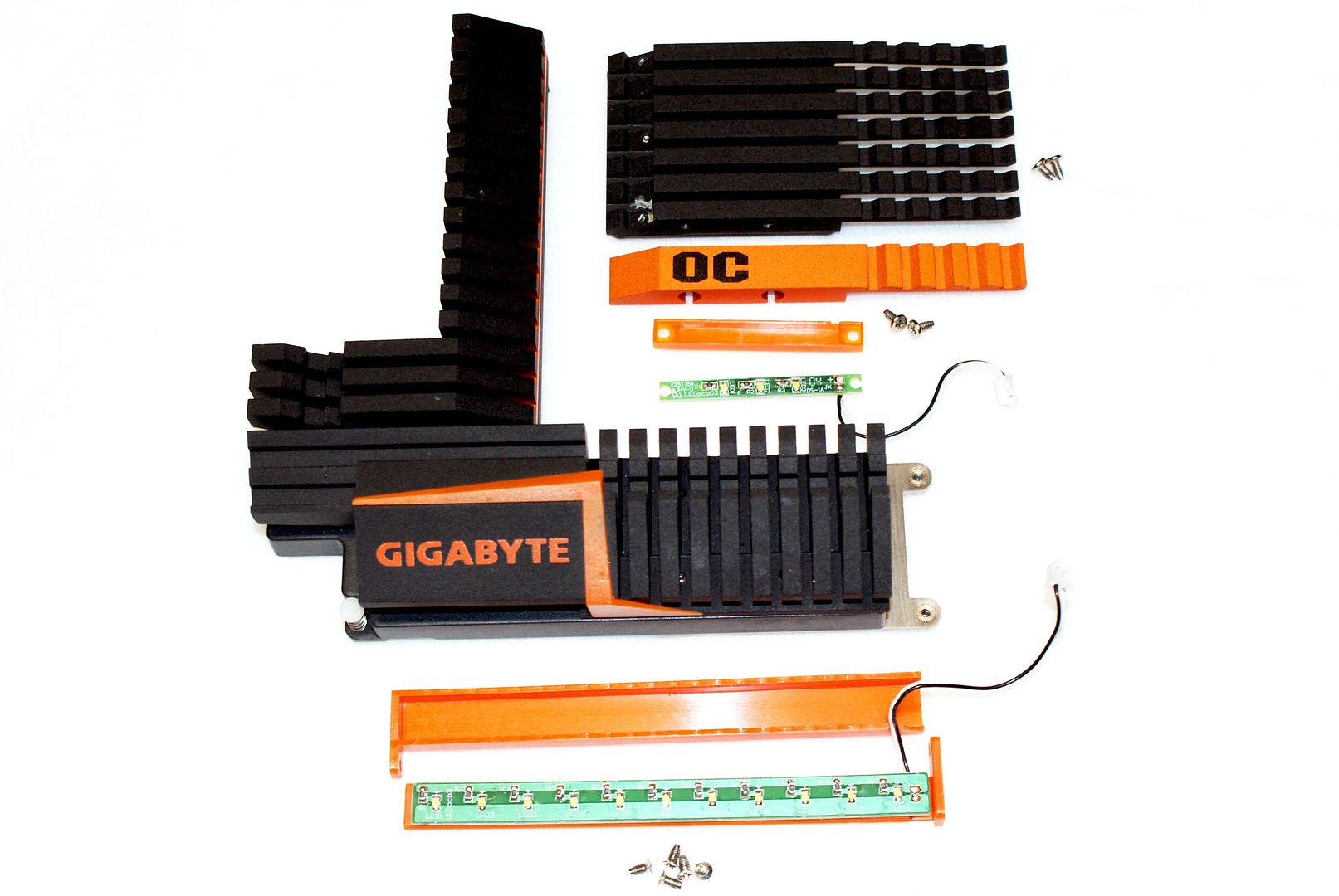
Motherboard Heatsinks:

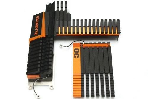
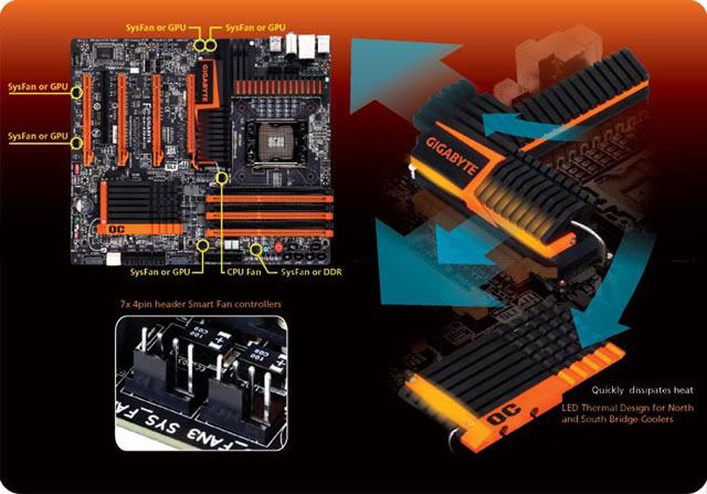
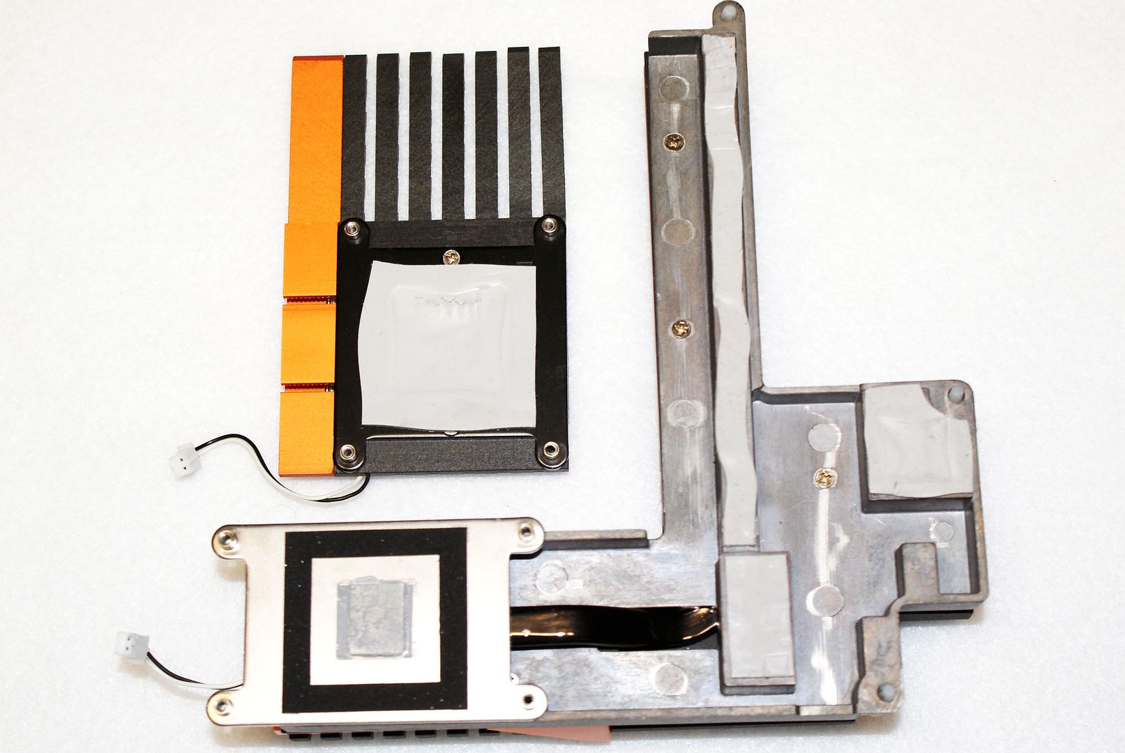
Heatsinks have been removed, you can see they all made very good contact, even the VRM section that was held with push-pins had good contact. This is a very hefty heatsink and it does a great job at cooling the MCH and VRM's down. It's finished in a flat black, with orange accents to match the board, and the orange trim in between the fins looks very cool in person which also matches it's actual cooling ability.
The "OC" Flag of the SB heatsink is removable, possibly for future use to be able to re-use this heatsink design with another color themed board(?) Both heatsinks have removable plastic sections housing orange surface mount LED's. There are three LED's located in the SB heatsink, and eleven in the MCH/VRM heatsink.
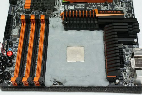
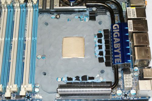
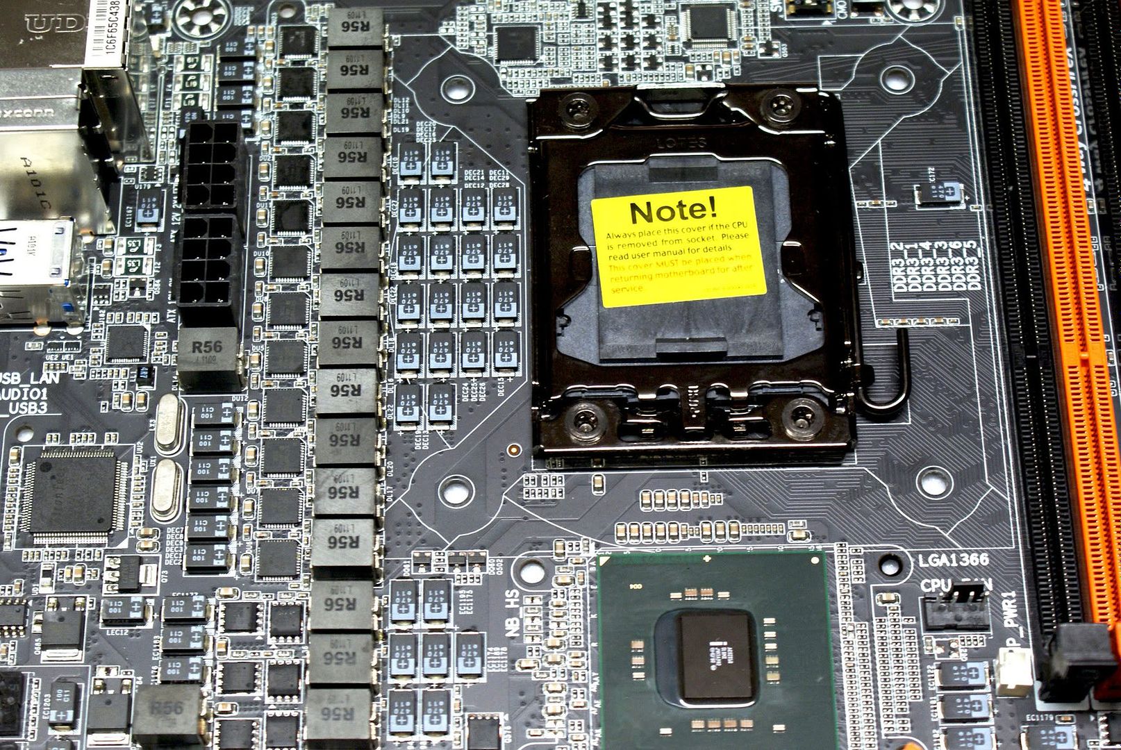
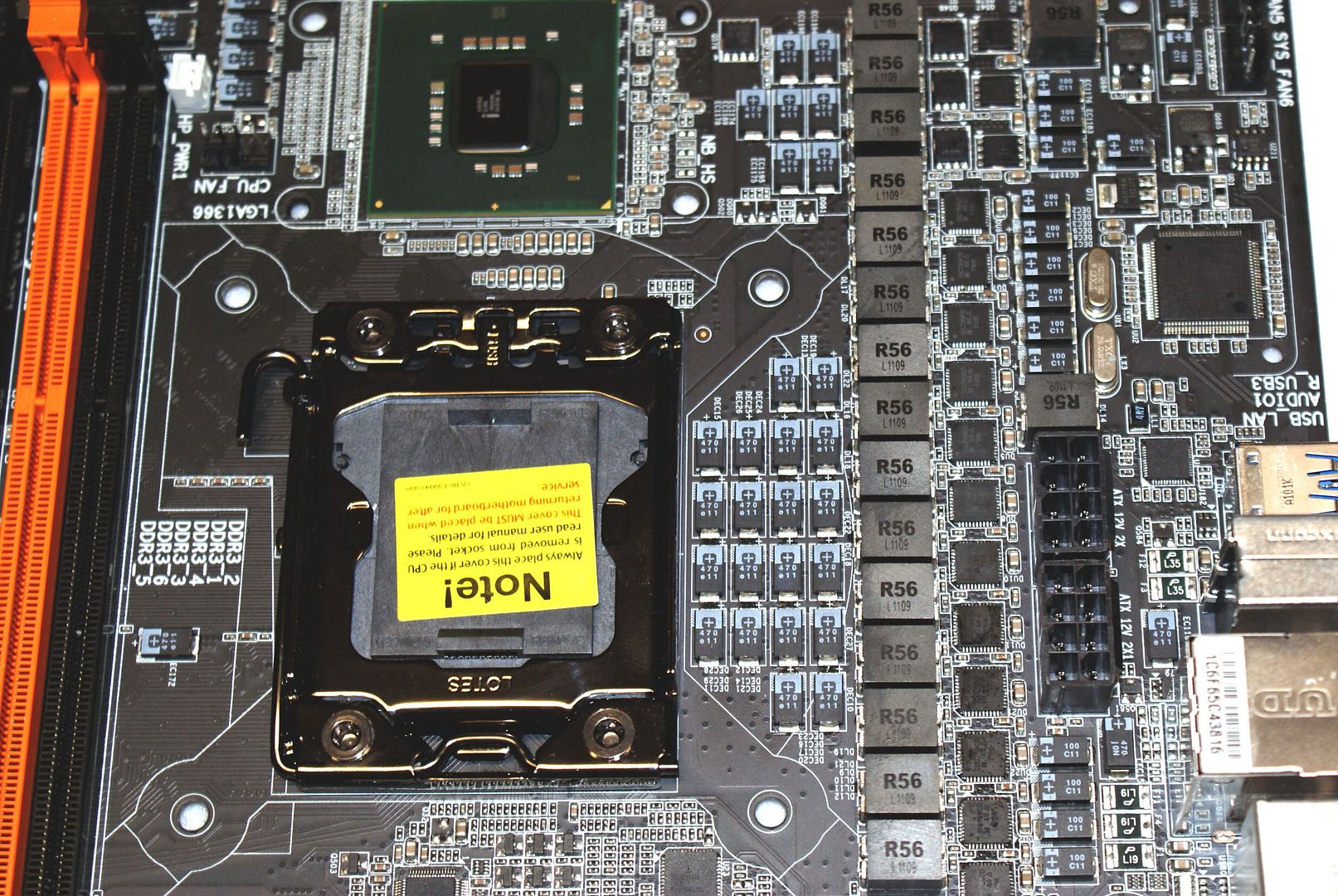
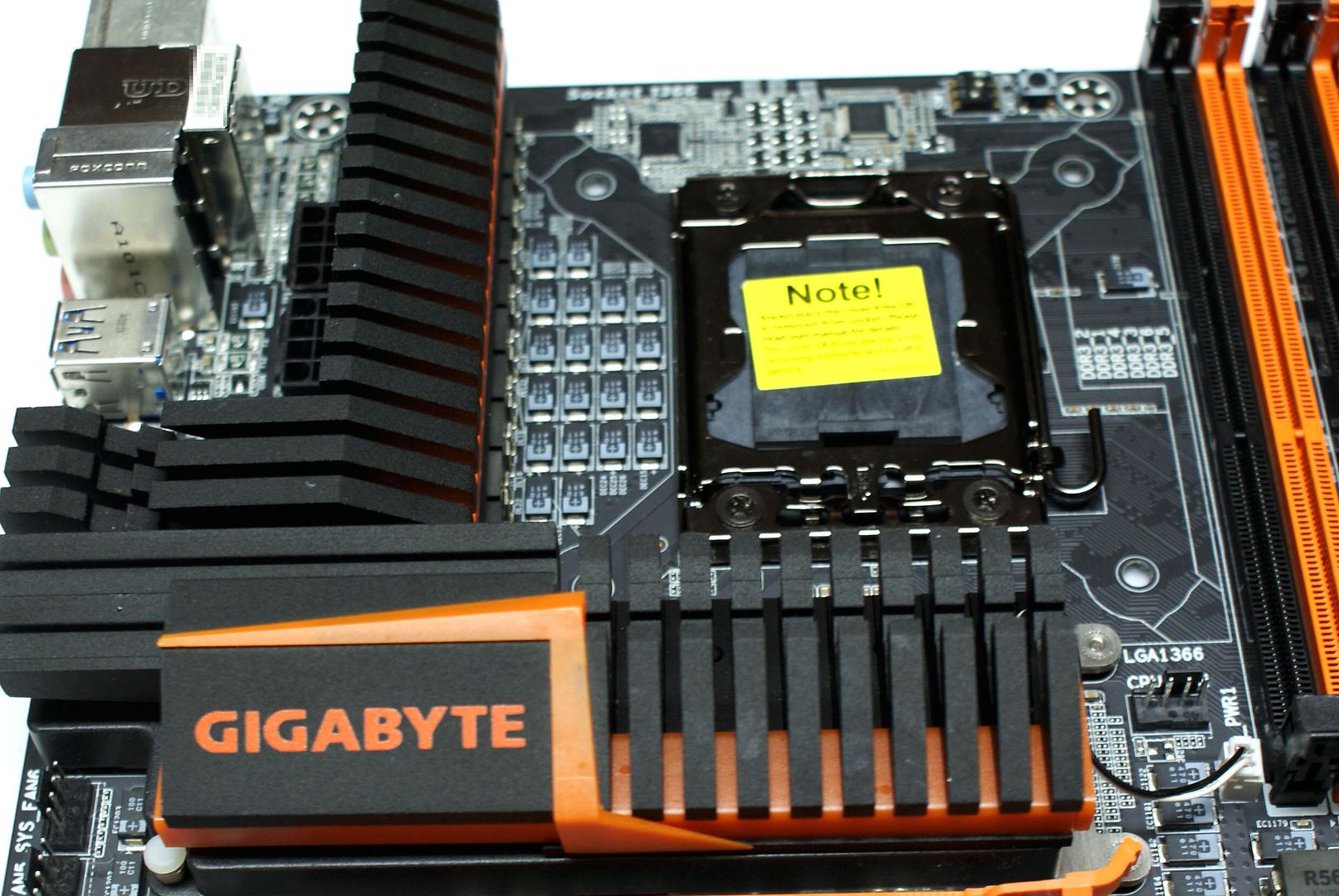
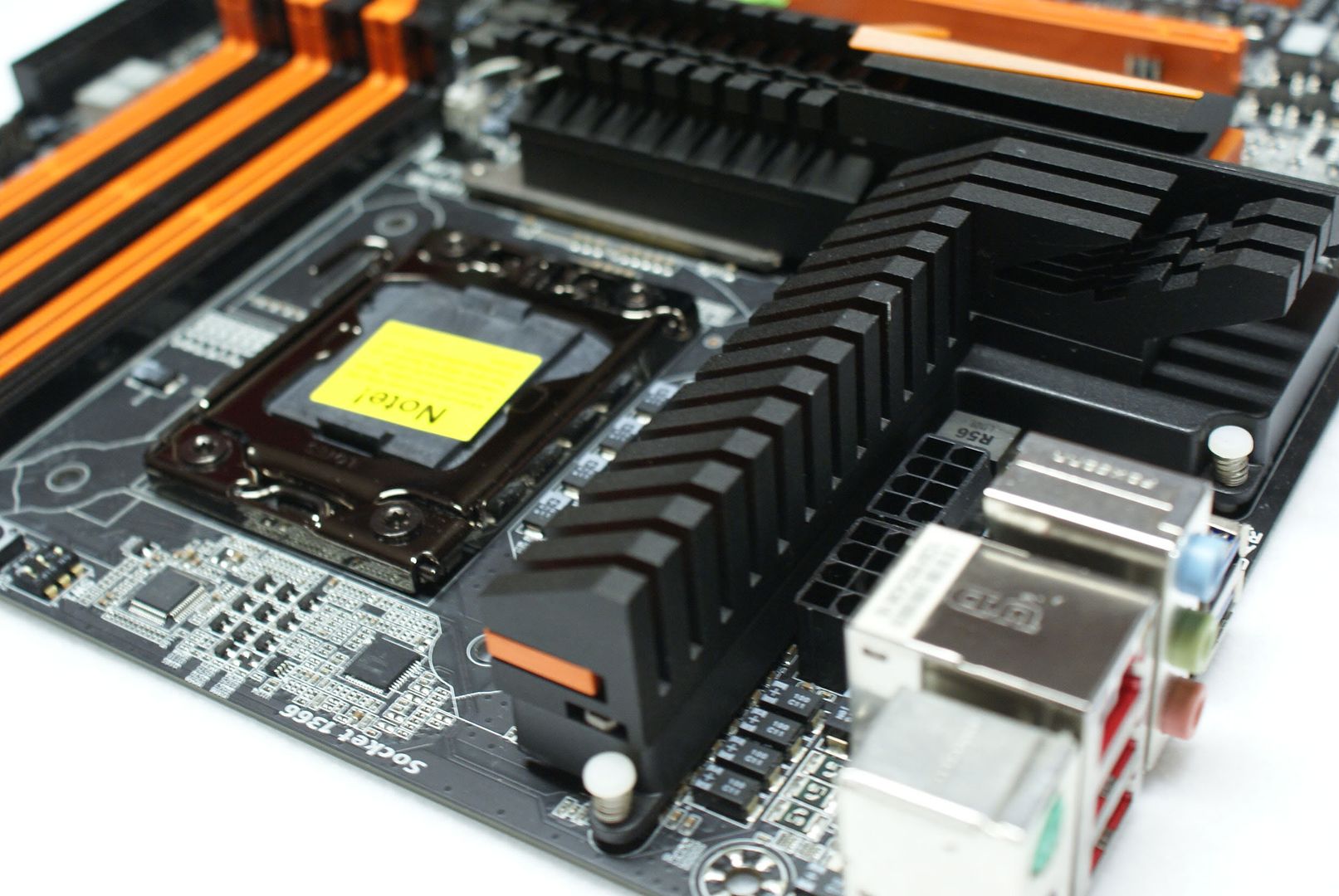
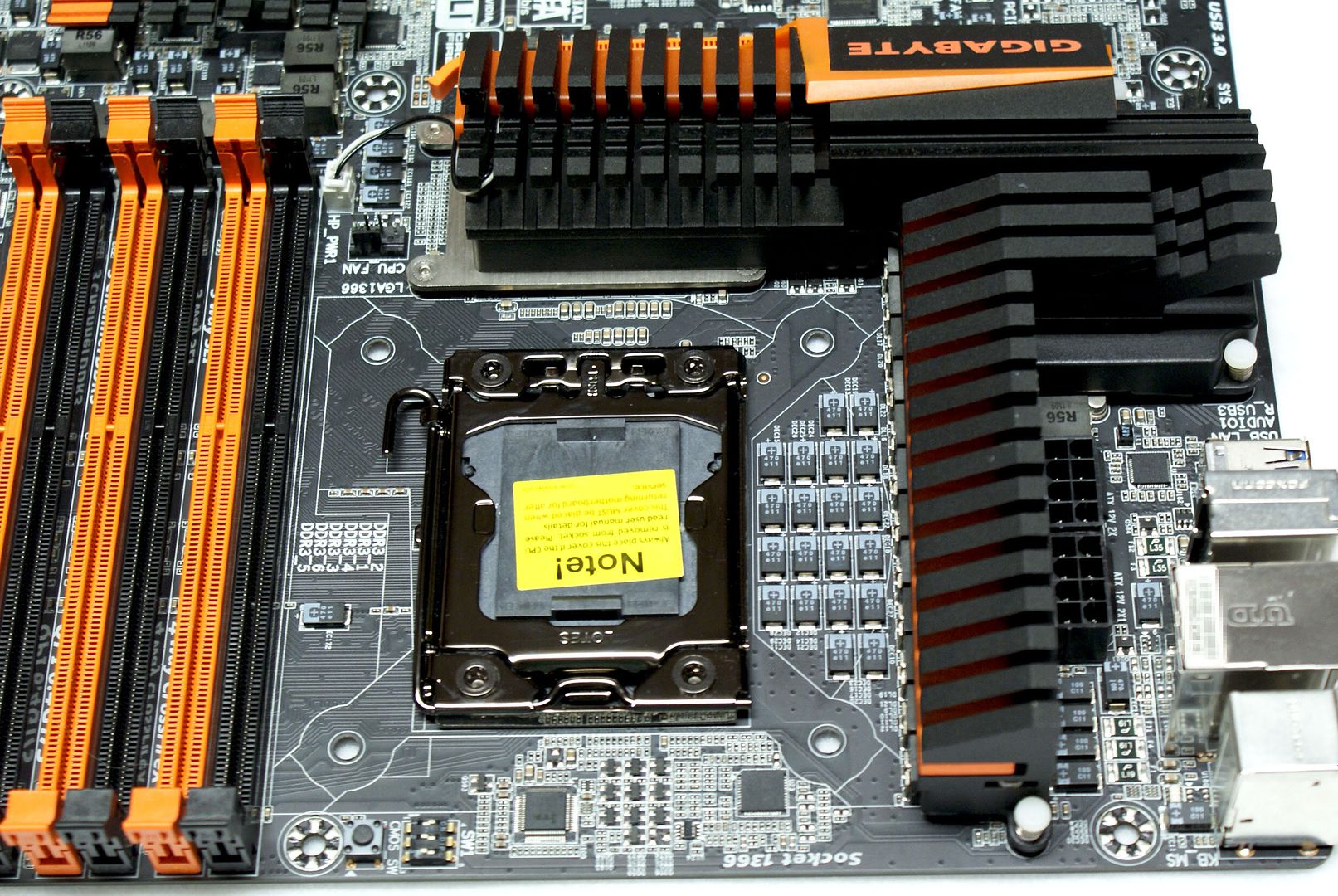
CPU Socket Area:
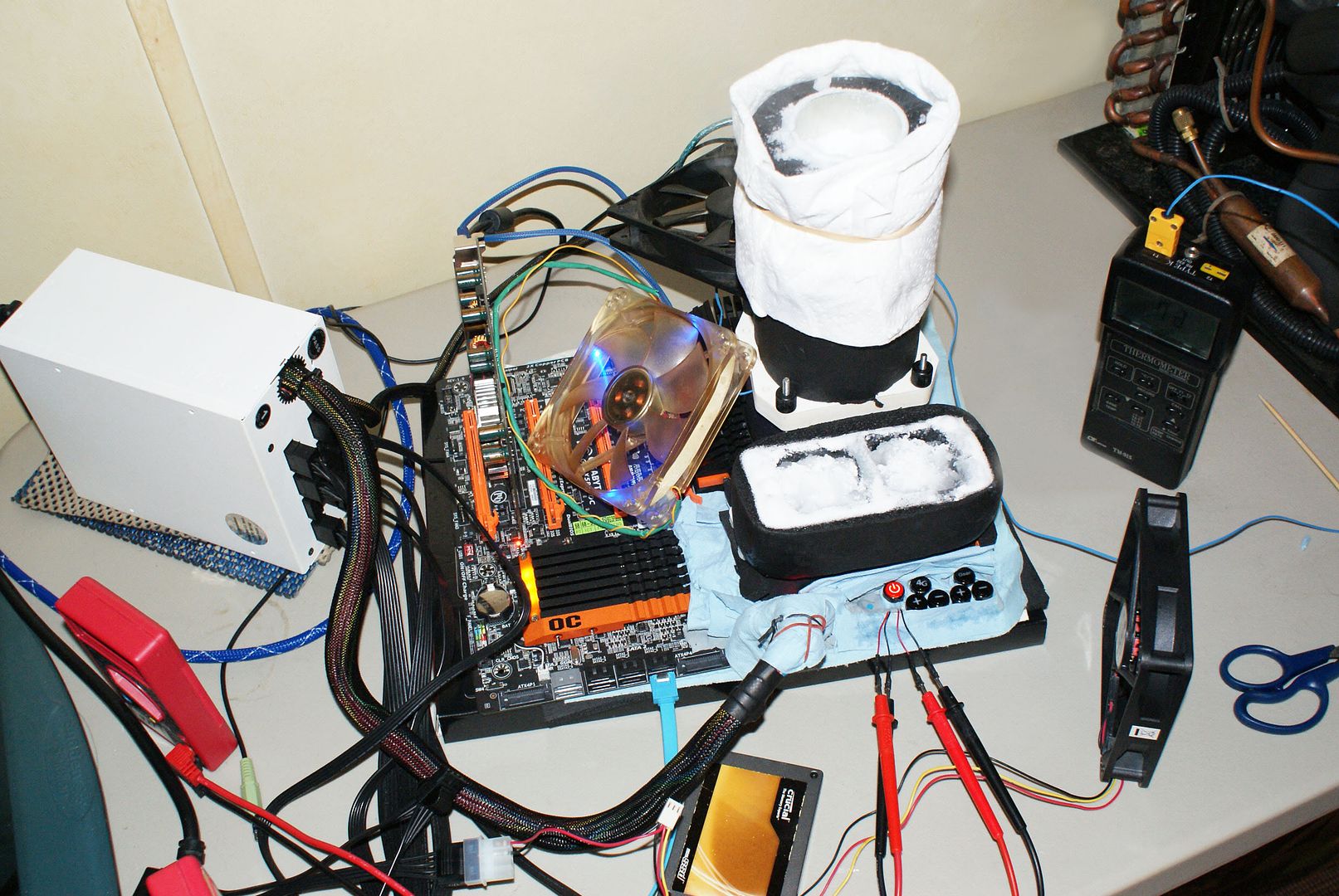
This board's CPU socket area means business, there is plenty of room to mount any LN2 or Dry Ice cooling pot!!
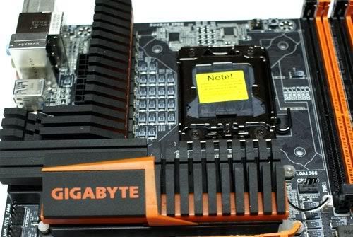

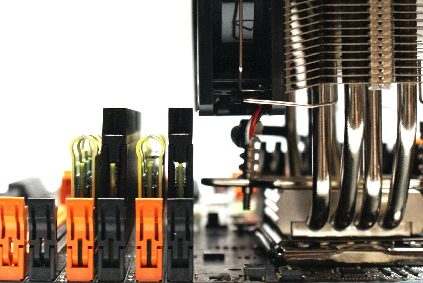
Showing the socket area from a few more angles, so anyone wondering about various CPU Air coolers can gauge a good estimate of fitment. I'll be showing a few air coolers mounted on this board later as well, for anyone that has any concerns about being able to fit their cooler.
SATA & PCIE Spacing:

The SATA ports are in the perfect position, they are easily accessible from the side of the motherboard, and their placement does not interfere with any of the larger graphics cards now available.
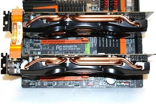
As you can see from these various angles, there is plenty of room for any dual or even triple slot graphics cards to easily fit. These are dual slot cards and they are not squeezed together at all, leaving plenty of room for the cards to breathe. Again the X58A-OC can run two-way Crossfire or SLI at x16/x16, or three-way at x16/x8/x8, and Crossfire with four cards can also be utilized at x8/x8/x8/x8 (ATI Only).
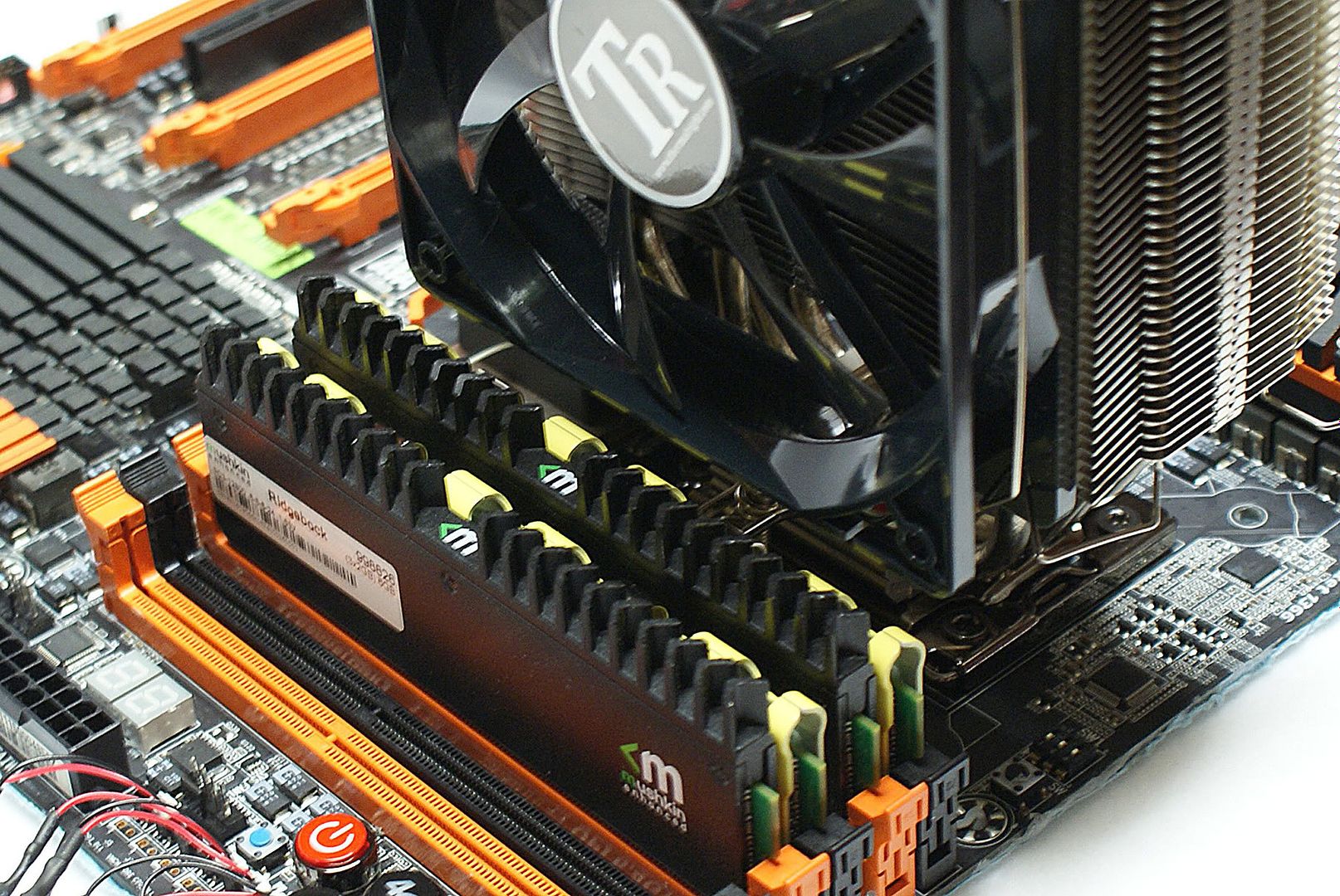
Memory Slots & Heatsink Fitment:
Heatsinks used:
Scythe SCSK-1100 100mm Shuriken Rev. B 3 Heat Pipes CPU Cooler
Fan Dimensions -- 100 L x 100 W x 12 H mm
Heatsink Dimensions -- 105 L x 116 W x 64 H mm
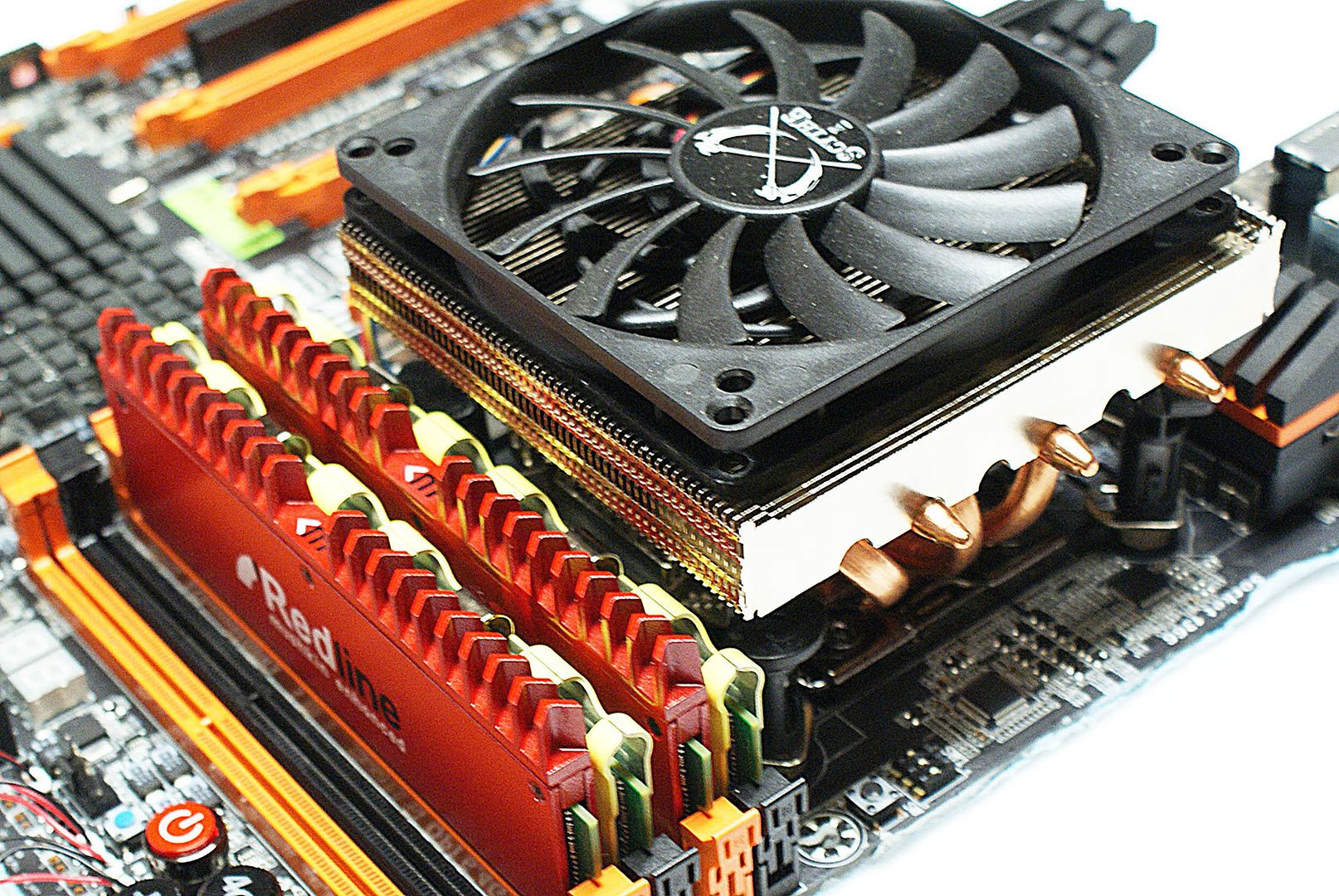
Thermalright MUX-120 Heatpipe CPU Cooler
Heatsink Dimensions -- 133 L x 58 W x 160 H mm
Fan Dimensions -- 120 L x 120 W x 25 H mm
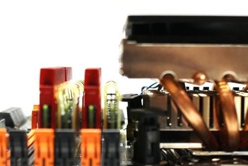
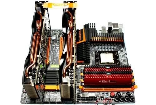
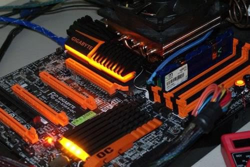
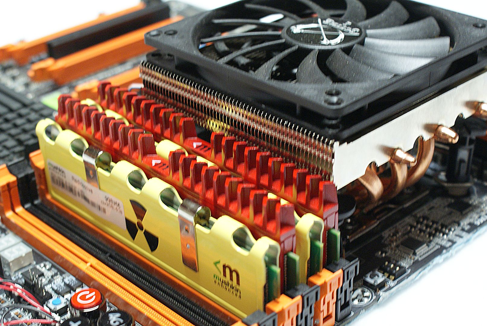
As you can see, even with this oddly shaped down-draft air cooler from Scyth, there are no issues with taller memory. If you have a similar cooler, and needed to mount the cooler with the heat pipes facing the memory, then that may cause issues depending on the cooler and memory you are using.

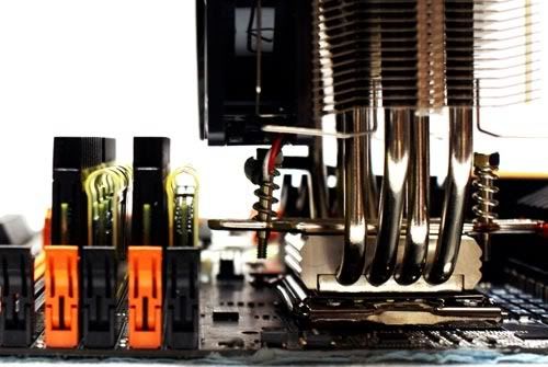
No issues with the Thermalright Mux cooler and taller memory either, as you can see there is plenty of room for even taller modules than the ones I used in these examples. Yes, that cooler is not actually mounted, as I did not have a 1366 mount for it, but it is in the proper exact mounting position, so for these purposes it is accurately depicting a mounted cooler.
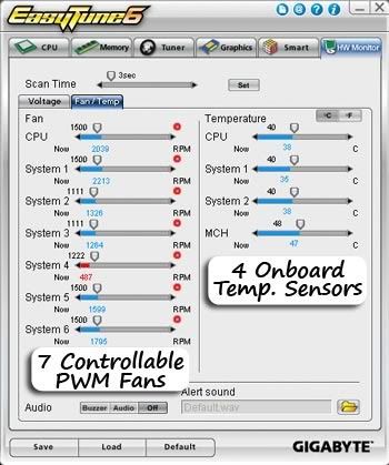
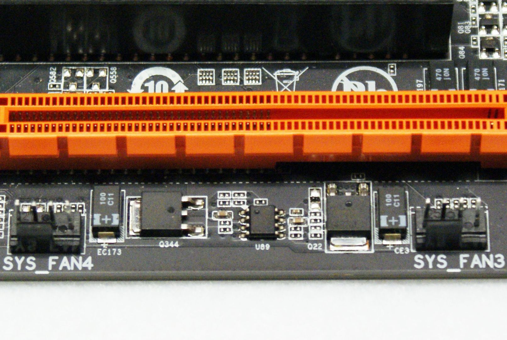
7 On-board PWM Fan Connections:
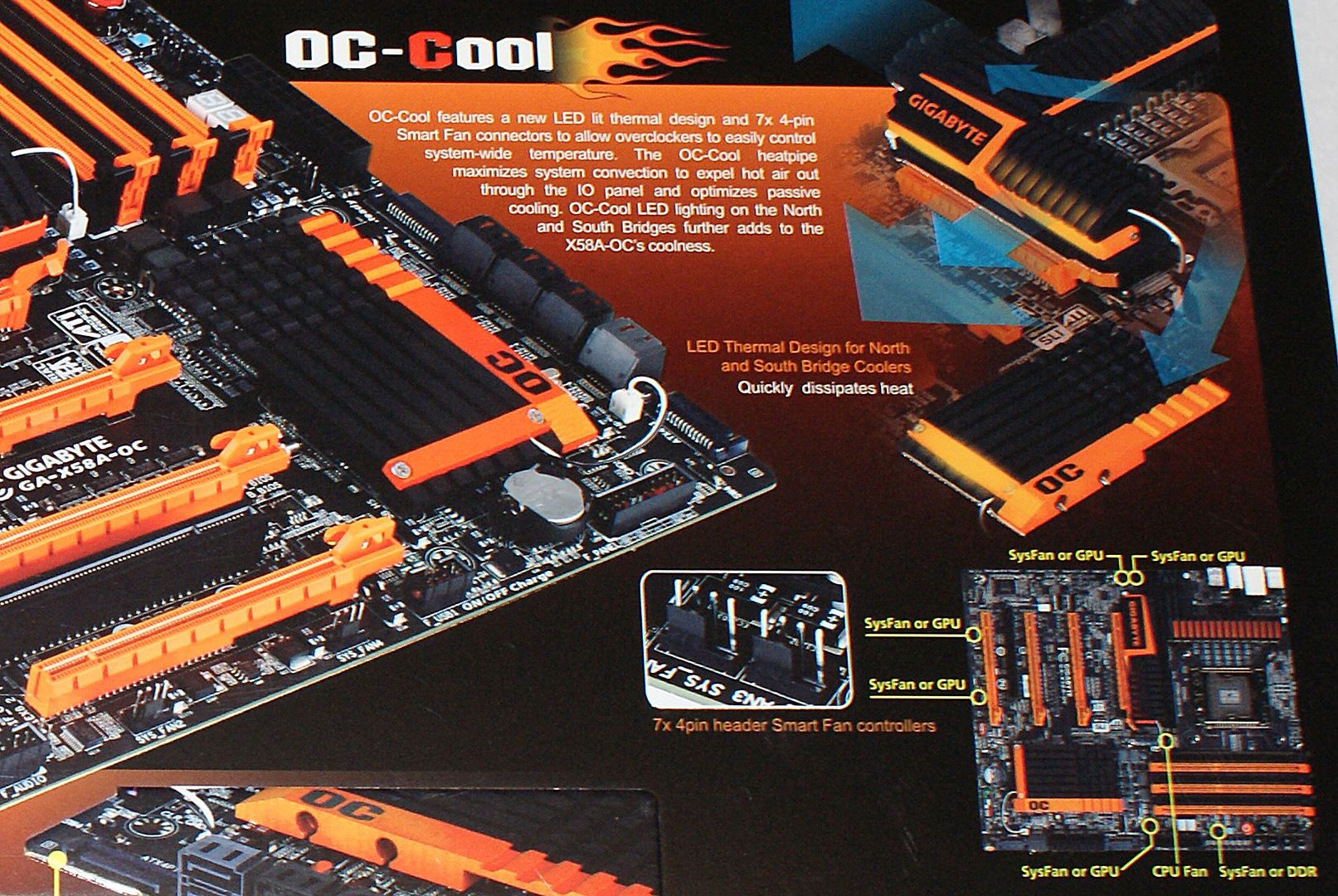
This motherboard offers some new fan and sensor features over GIGABYTE's other X58 models, this board has 4 on-board temp sensors, and 7 user controllable PWM fan connections. You can set the CPU's PWM fan slope in the BIOS manually, the other fans would need to be auto controlled via the PWM controllers, or set by Easytune or Speedfan.

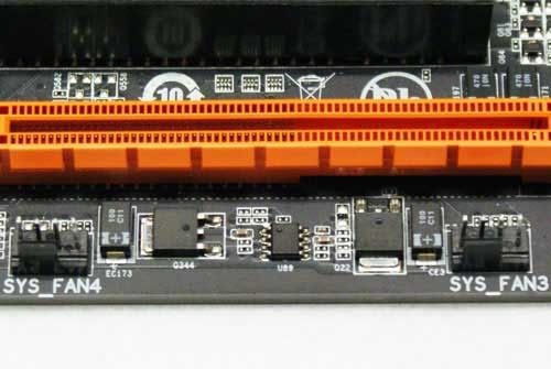
Here you can see the locations of the many on-board PWM fan connectors, they are conveniently located at various positions across the board. There is also an additional 3 pin NB fan header not shown here, so that's a total of 8 on-board fan headers!
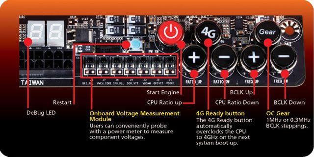
On-board Buttons, Switches & Unique Connectors:
Hey, haha, it's a morphing .gif!! I'm far from being a graphic professional, as you can tell, so don't laugh too hard - just wanted to add a little humor somewhere (very little).
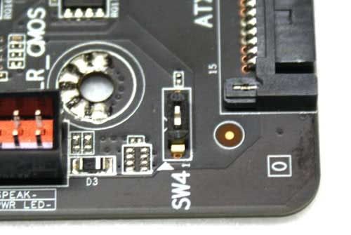
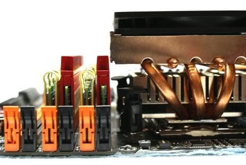
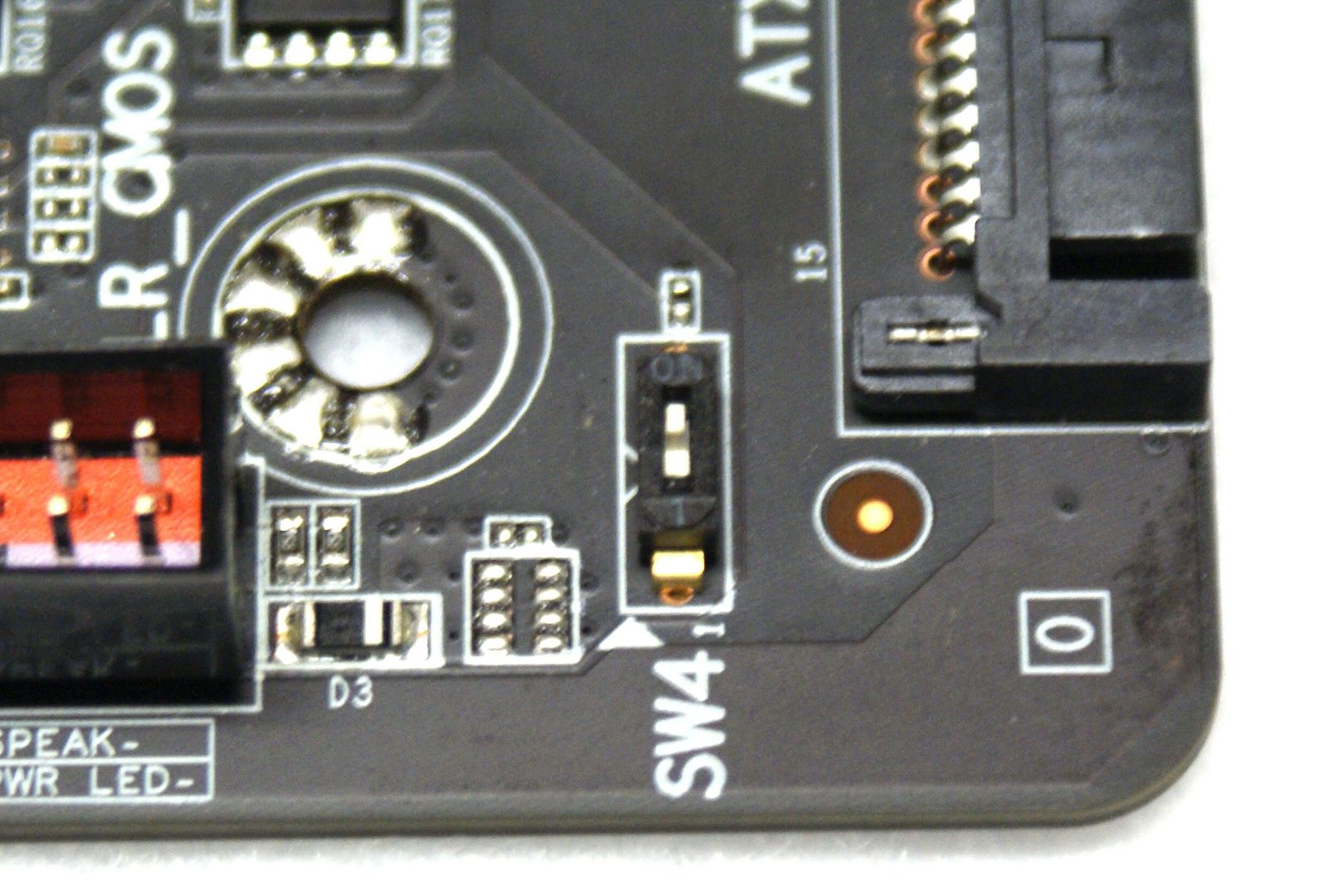
The image on the left is showing the BIOS switch (OC-Dual BIOS), located in the lower right corner of the board near the front panel header connections. This allows you to switch to booting from one BIOS to another, Backup BIOS or Main BIOS. Please be sure you power down the board before switching!
On the right we have the Clear CMOS button, and the CPU PWM Frequency switch that is part of the OC-VRM feature set. The PWM Switches allow you to set the PWM phase switching frequency to 600K, 800K, or 1000K, the default with all switches in the Off position is 400K.
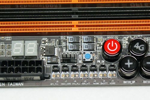
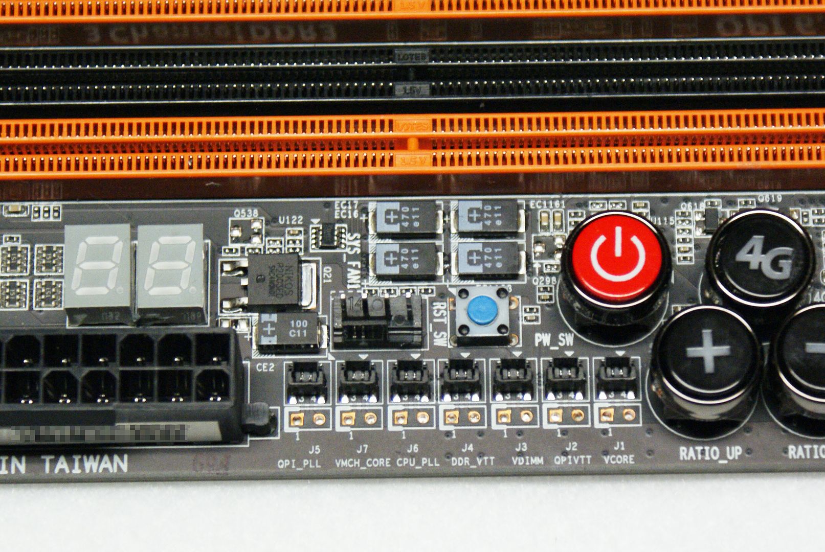
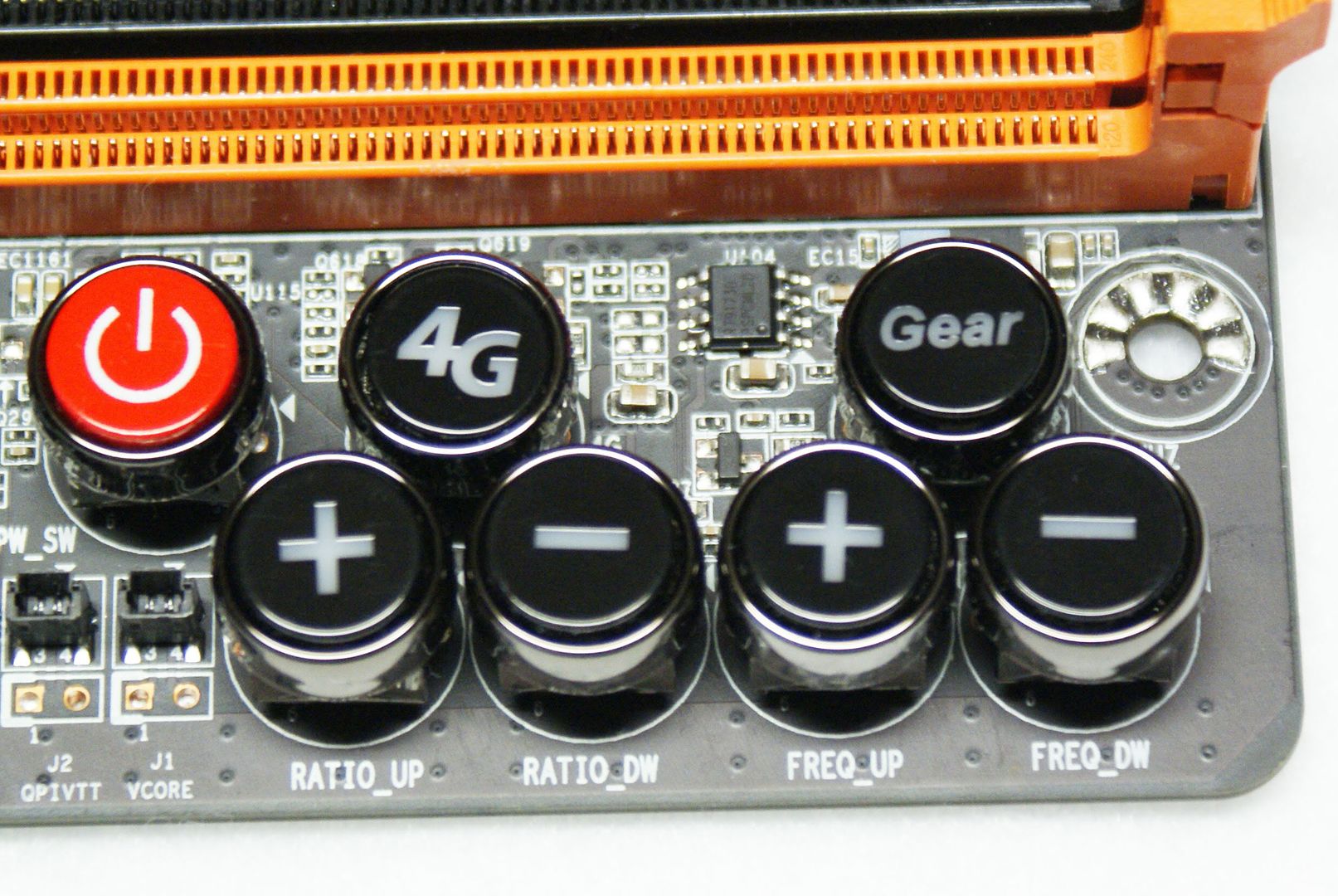
Here you can see the power and reset buttons, the on-board debug LEDs, and the on-board voltage readout connections and points. These voltage readouts are part of the OC-Touch feature set, and you may either connect one of the voltage readout cables to connect to your DMM to view current voltages, or you may use the "Touch" points directly on the PCB just below the wire connection points.
On the right you can see one of the OC-PEG SATA power cable connections, there are two of these, one on each side of the SATA data bundles. These are designed to connect to a SATA power cable from your power supply to deliver a better electrical signal to the graphics cards, thus delivering a more stable graphics overclock, especially when using 3 or 4 graphics cards.
The debug LED will be one of the cons I'll be listing later in my final thoughts. The location of the debug LED is not ideal, it is not visible from almost any angle once you have everything setup and running. The only way to view the debug LED while benching, if you have any issues and needed to check, would be to either stand up and stand over the board, or already have it setup so that you are north of the top end of the board. It is not visible from while looking at the board from an angle, not visible if you are sitting below the bottom end of the board, and not visible if you are beside the board horizontally. I would imagine that it may be visible with the board in an upright position (such as in a computer case), that is if your 24pin ATX cable wouldn't also be blocking it, however, this is a benching board so having it in a case contradicts the intended purpose.

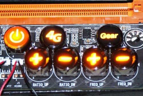
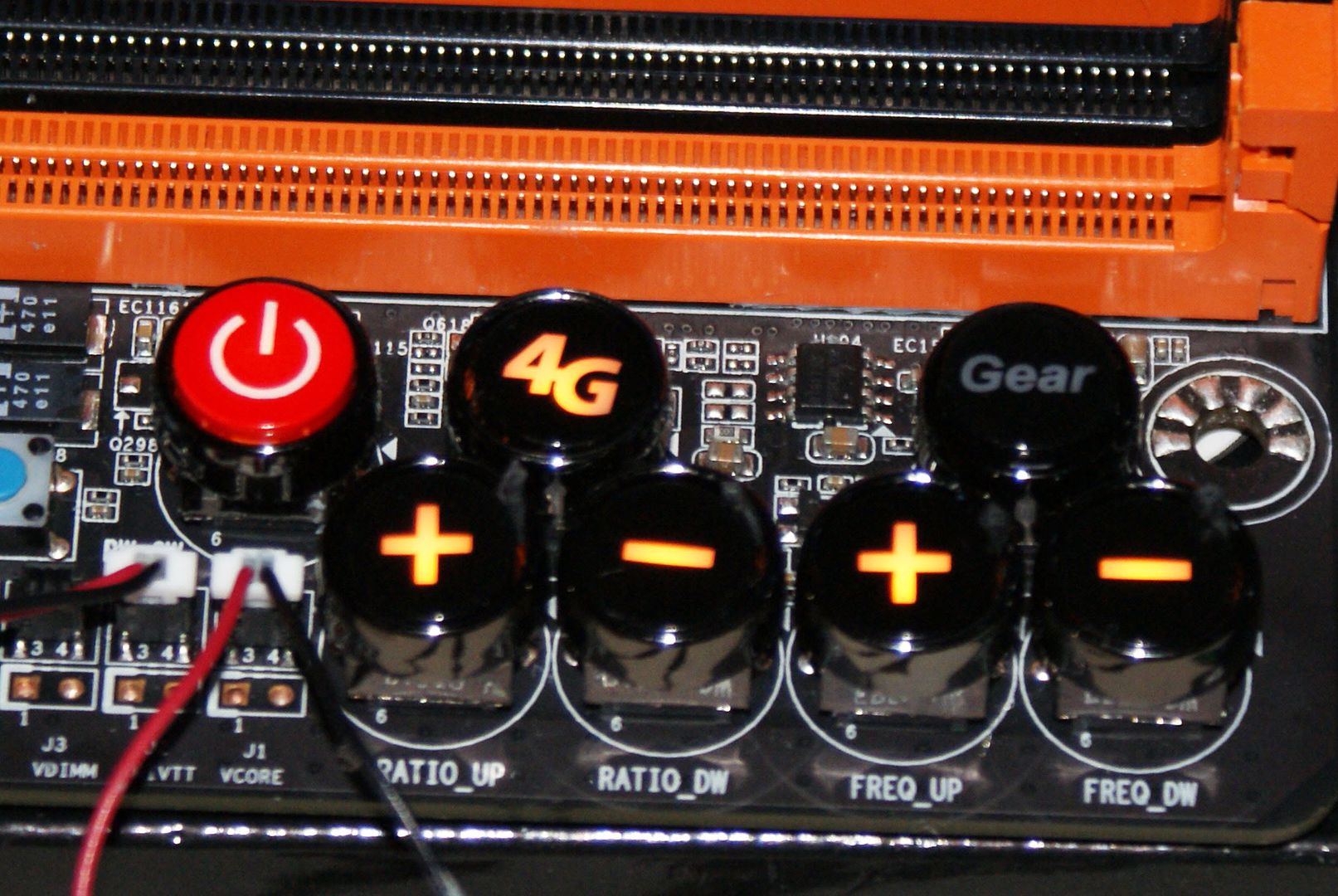
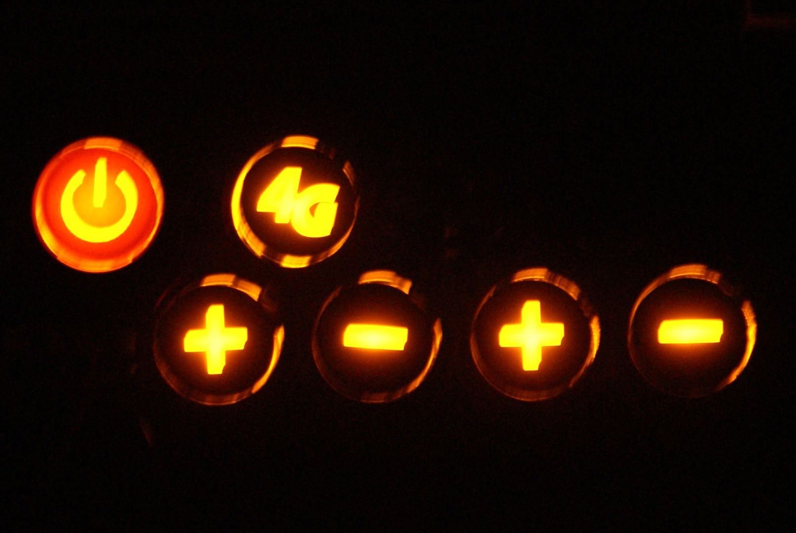
These are the on-board CPU frequency buttons, part of the OC-Touch feature set. The upper images are with no flash, and the one on the right is with the board powered on. The lower two images were both taken in the dark, one with flash and the other obviously without. The +/- buttons do not remain lit as you see them, they are only lit when pressed, I forced them to stay on for these images. The 4G button should only be pressed after loading optimized defaults in the BIOS, and then on reboot the system will load at 4Ghz. I had no issues with this function, and tested it on two CPU's, both of which booted to Windows at 4GHz and remained completely tested stable.
The gear button changes the +/- Bclk button to adjustments of either 1 Bclk or 0.3 Bclk, whichever you choose to use, and I found both to be VERY helpful to use while pushing for maximum Bclks, or to gain that few extra MHz while at very high CPU speeds.
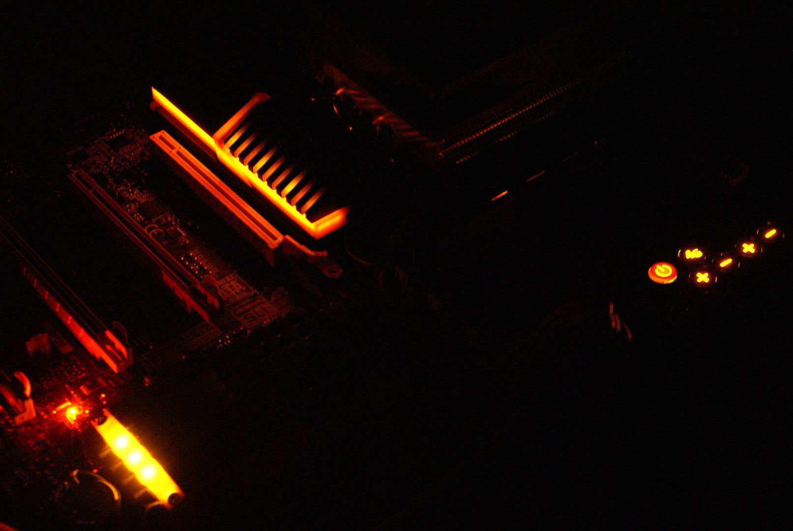
The last images both show the board in the dark so you can see the on-board LED's in action, left side with flash and right side without.
BIOS Examples:
The X58A-OC BIOS is exactly the same as most of the other GIGABYTE award based BIOSes for X58 motherboards, the only differences are that a few settings are disabled by default for overclocking, the CPU temperature reading in the PC health section reads much lower negative temperatures than other BIOSes, and finally there is a new CPU PWM fan adjustment setting adopted from the Z68 BIOSes.
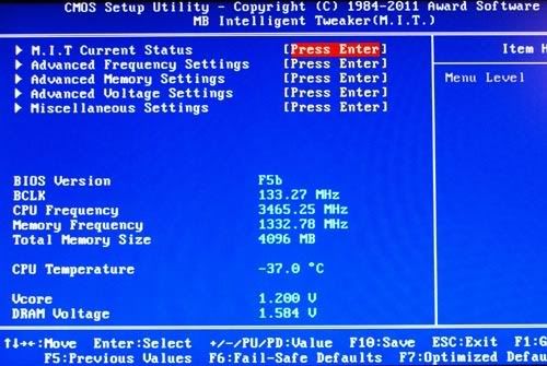
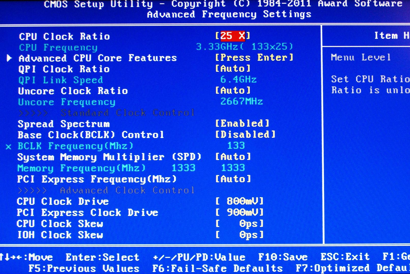
On the left is the main section of the M.I.T Overclocking section of the BIOS. This page offers entry into several sub-sections for further advanced settings, shows current CPU and ram voltages, along with the BIOS version in use and various current system frequencies. On the right is the Main Advanced Frequency settings, this has your CPU Multiplier, QPI, Uncore, Bclk, and memory adjustments and a sub-section to enter which is shown below, offering your turbo and power adjustment settings.
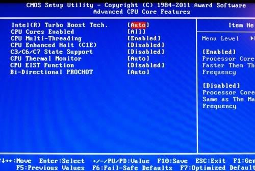
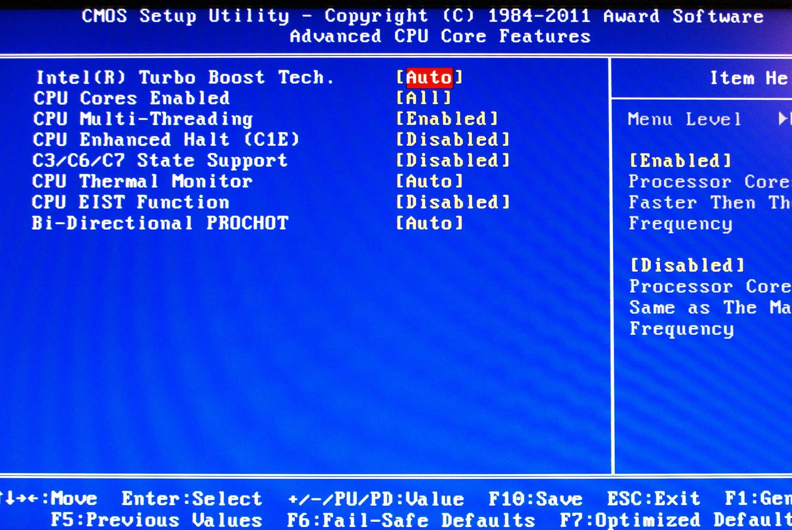
These are the default disabled settings of the OC's BIOS for the advanced CPU core features. Speedstep, and all power saving features are disabled by default in this BIOS. On the right you can see the upper half of the PC health section of the BIOS, this shows various current voltages, and 4 system temperature readings including the CPU readout which, as you can see, goes well below many of the past BIOSes. Other BIOSes stopped reading at -15c or -20C - if I recall correctly.
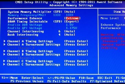
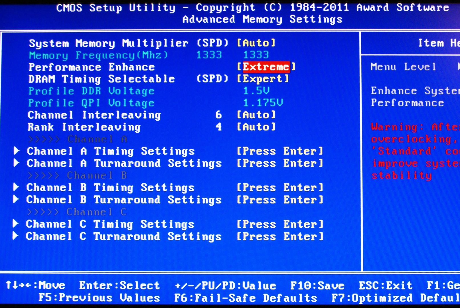
On the left here are your general memory settings, offering to enhance memory performance automatically, enable XMP or not, and to set the memory multiplier here if you wish instead of on the main frequency page shown previously. From here you also enter the main memory timing pages as shown on the right, which offer many various memory timings and sub-timings.
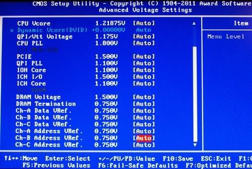
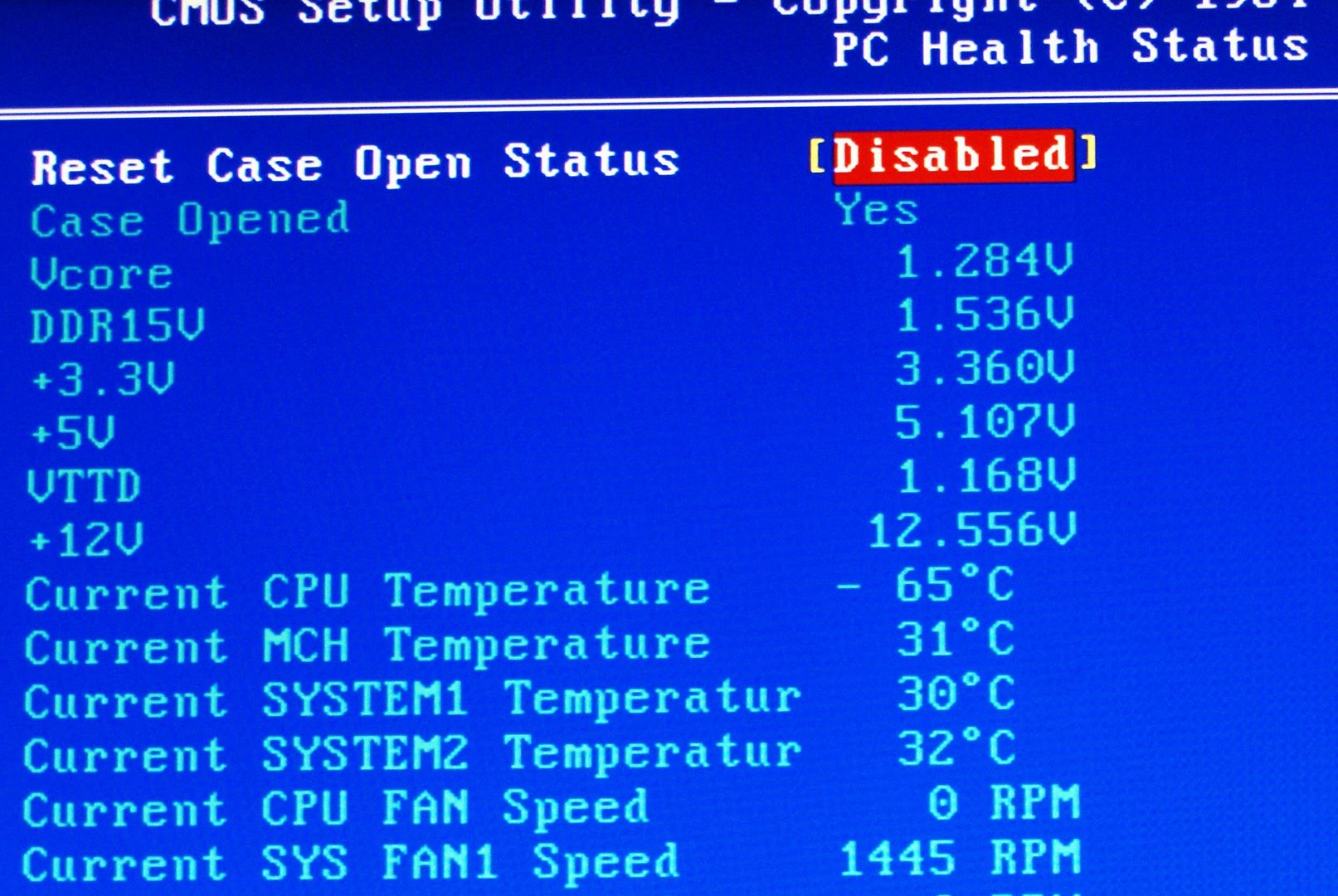
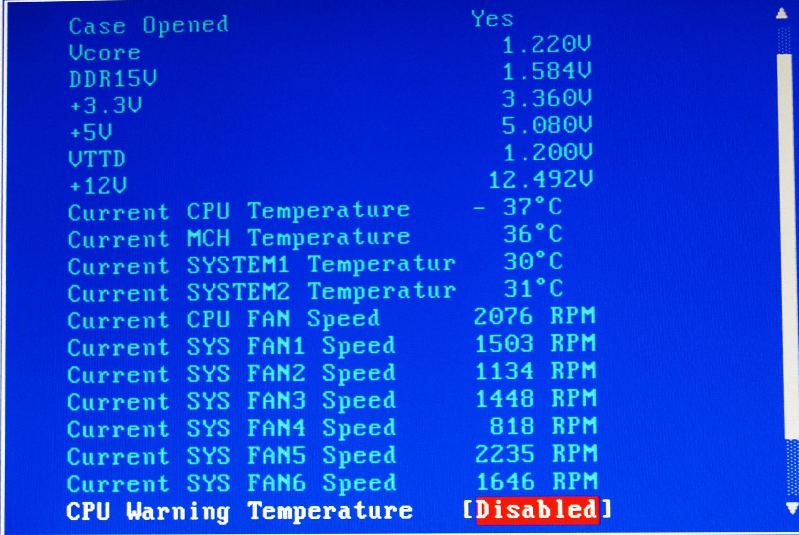
This is the main voltage setting page, offering Load Line Calibration (Auto, Standard, Level 1, and Level 2). You also have all your other voltage settings here such as CPU Vcore, Vtt, PLL, and memory voltage, as well as several other voltages to be adjusted. On the right you can see a complete view of the PC health section of the BIOS, showing the current voltages and temperatures, as well as the speeds of 7 fans (If in use).
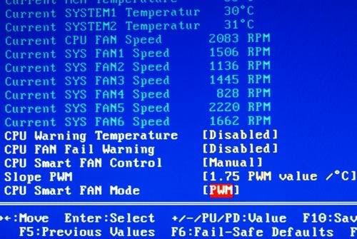
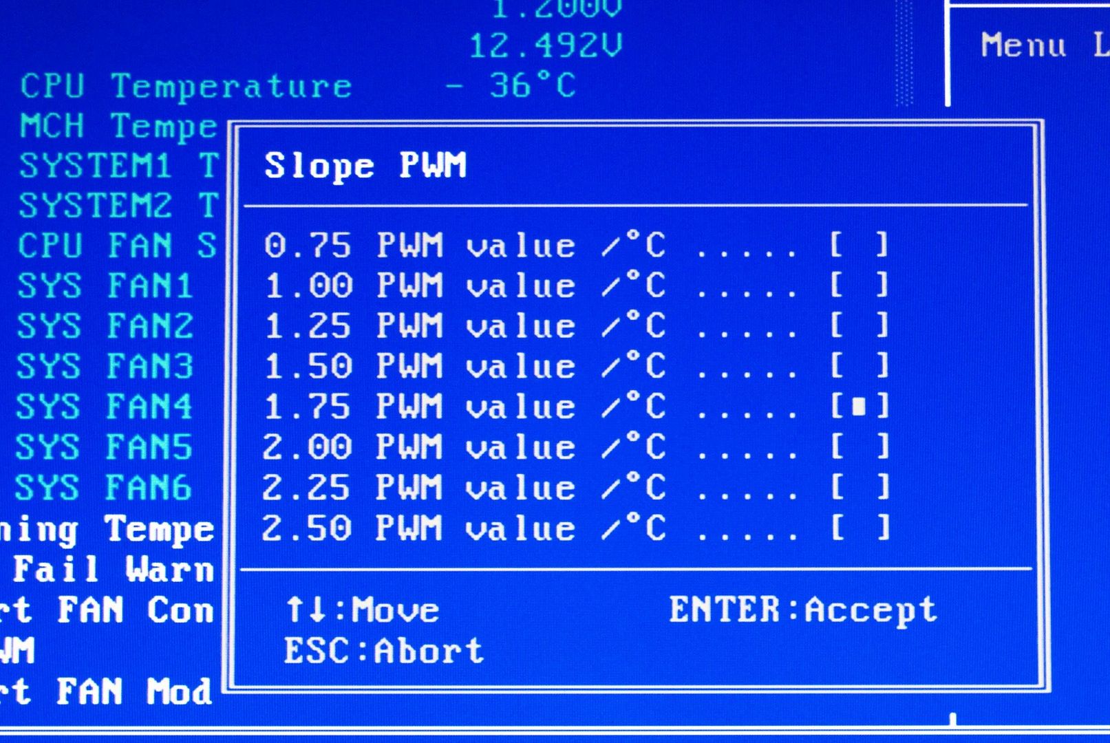
On the left you see the new PWM CPU fan voltage adjustment settings, you can set manually or use auto to adjust the PWM value, and set per voltage or PWM. On the right is the actual manual PWM CPU fan adjustment choices, I believe these are in percent of PWM value / temperature.
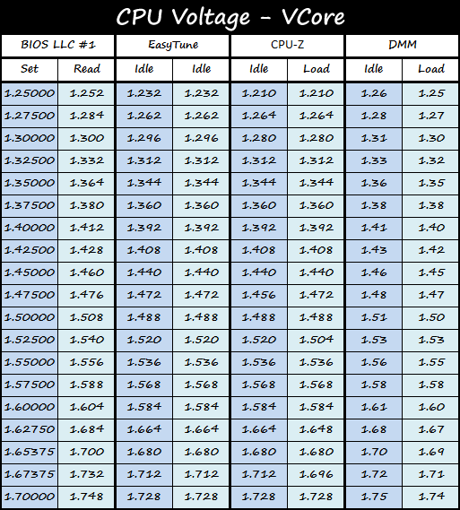
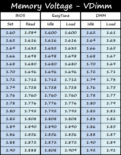
Measured Voltages:
For all voltage testing performed F5b BIOS was used, and the CPU was set to 3.6GHz while cooled using phase cooling, Load Line Calibration was always set on Level one throughout all testing.
Each voltage adjustment was done in the BIOS, and the idle measurements were recorded 5 minutes after Windows had loaded and set idle. The load was produced using Prime95 blend and ran for 10 minutes each round before a load voltage measurement was recorded.
Vcore
As you can see the actual delivered Vcore using LLC Level 1 is very close to what is set in the BIOS. Actual voltages being only a small amount higher at idle, then closer to the exact set amount under load except when you get towards the higher end of the voltage options (Where it continues to raise above the set amount exponentially).
Memory
Memory voltage on average proves to be around 0.02V higher than what is set in the BIOS, and then under load droops to only 0.01V over what is set in the BIOS. Anyone sticking to a 1.65V memory voltage should use 1.64V on the OC board.
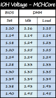
CPU Vtt & IOH
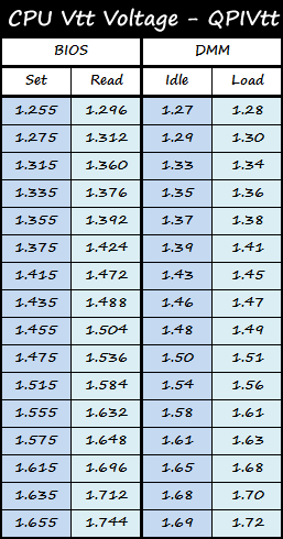
Much like the memory voltage, CPU/QPI Vtt voltage is higher than what you set in the BIOS, by 0.02V-0.03V on average, and this amount increases by an additional 0.02 on average under load, therefore the eventual load voltage is actually 0.25V-0.5V more than set and this increased more as the higher voltages are used.
IOH voltage proves to be a steady 0.05 higher than set in the BIOS, drooping under load very few times to just under the idle amount.
All in all, the OC board offers very stable and dependable voltage amounts. Once you know what to expect, from the amounts you set in the BIOS, the voltages will remain constant as you carry out your benching sessions
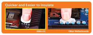
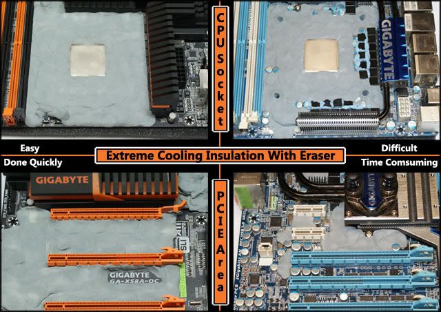
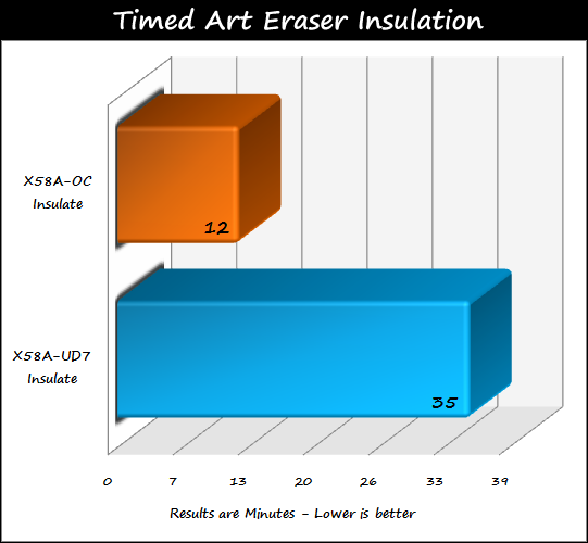
Extreme Overclocking Insulation Comparison:
As you can see, the X58A-OC motherboard is much easier to insulate the board when using eraser compared to other boards, the same would apply with other insulation methods such as Dragon Skin, liquid electrical tape, ect.
GA-X58A-OC motherboard
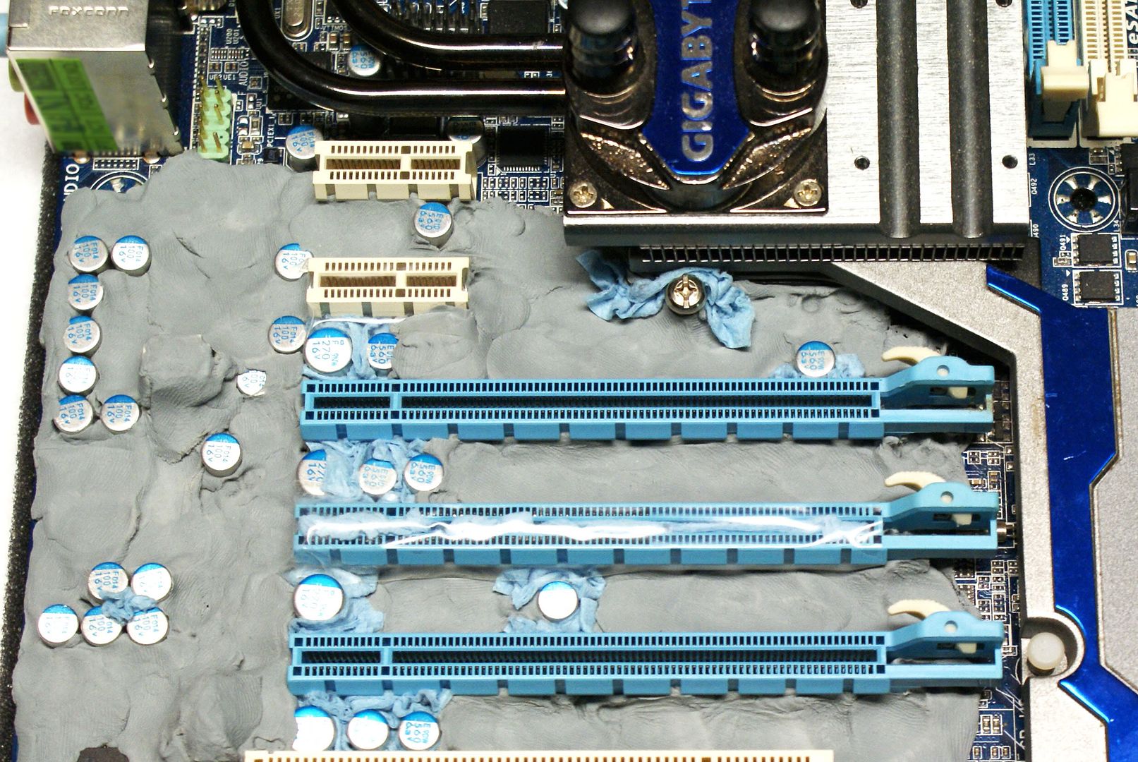
The CPU socket area, and the PCIE areas on the OC motherboard are very simple to insulate, thanks to the use of POSCAP capacitors across the board. This drastically cuts down the time required to insulate and prepare the board for freezing, which saves a lot of time normally spent for this process that can now be used for actual benching instead!
GA-X58A-UD7 Motherboard
Insulating a motherboard that has common barrel type capacitors is much more difficult, as you can see here on the UD7 motherboard. Insulating any board similar to this also takes significantly more time to complete, which cuts right into your precious benchmarking time.
As the graph indicates, insulating the OC motherboard takes less than half the time it took to insulate the UD7 board, making the X58A-OC ideal for benching sessions where time is normally of the essence.
X58A-OC Vs. X58A-UD7 Testing
Hardware Used:
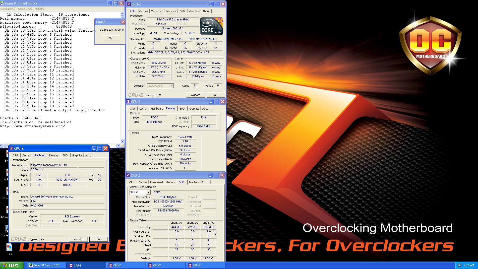
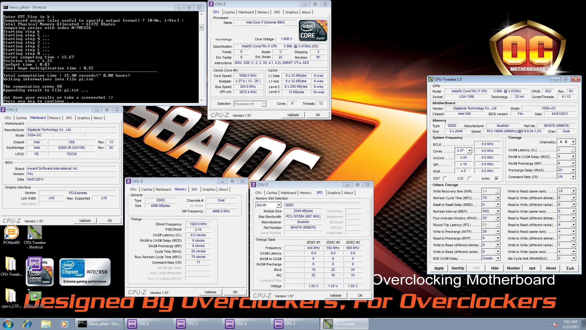
GIGABYTE GA-X58A-OC Motherboard (F4c & F5b BIOS - Mainly F5b)
GIGABYTE X58A-UD7 Motherboard
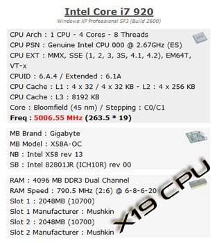
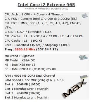
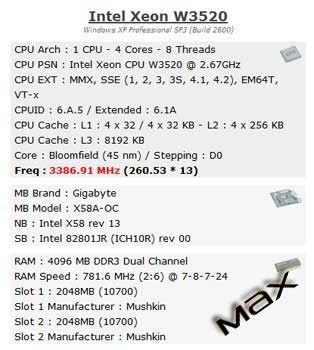
Intel Quad & Hexa Core i7 CPU's - i7-920, i7-965, i7-980X & i7-990X
Mushkin Memory - Blackline 998679 (Used in main comparison), Ridgeback 998826 & Radioactive 998966 ~ (4GB used by choice for benching purposes)
GIGABYTE HD5870 1GB Super Overclock (SOC) Edition Graphics Card x 2
PNY FX 5500 - 128MB PCI Graphics card (Bclk Benching)
Crucial RealSSD C300 128GB Solid State Drive x 2
NZXT Hale90 750W 80+ Gold Power Supply
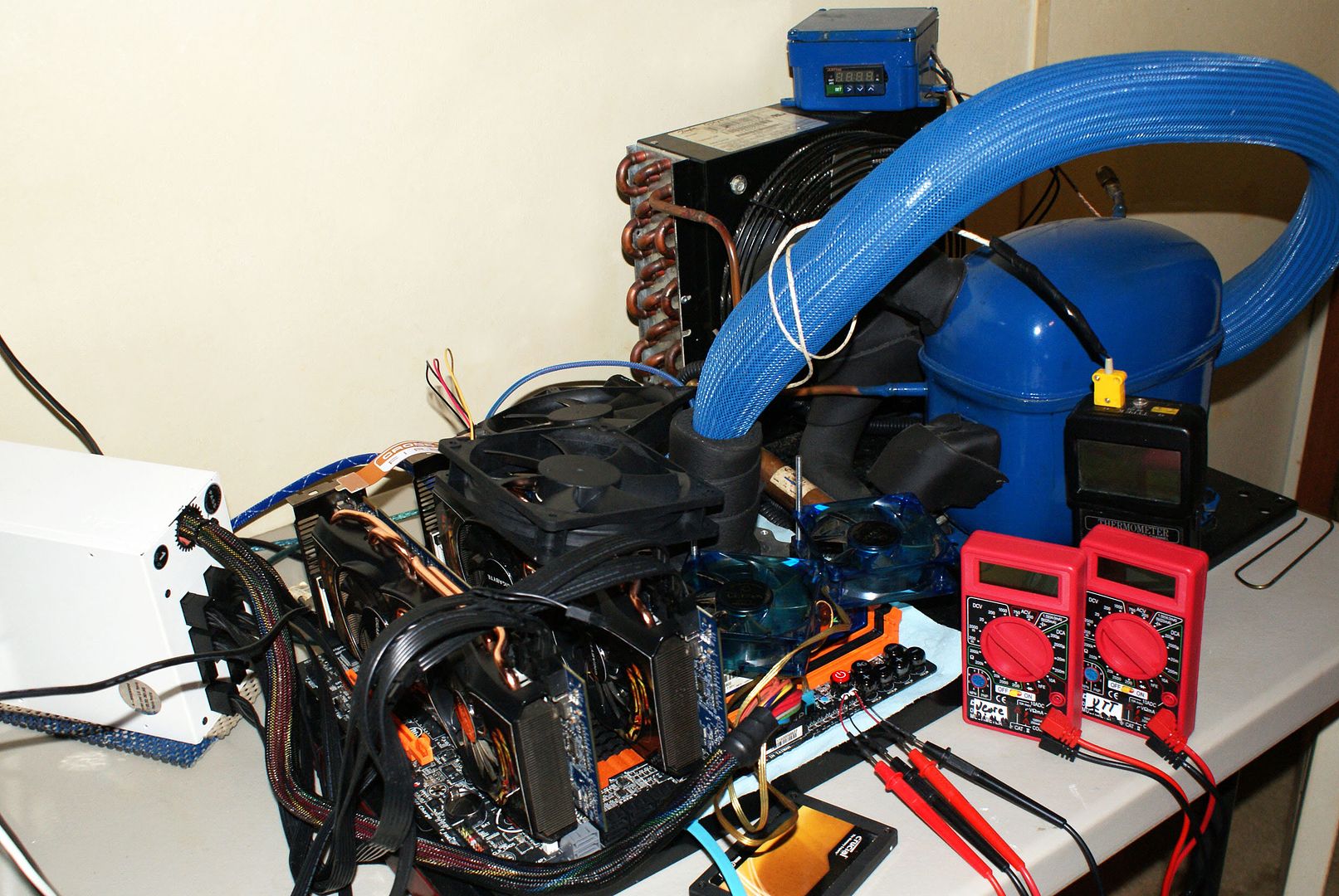
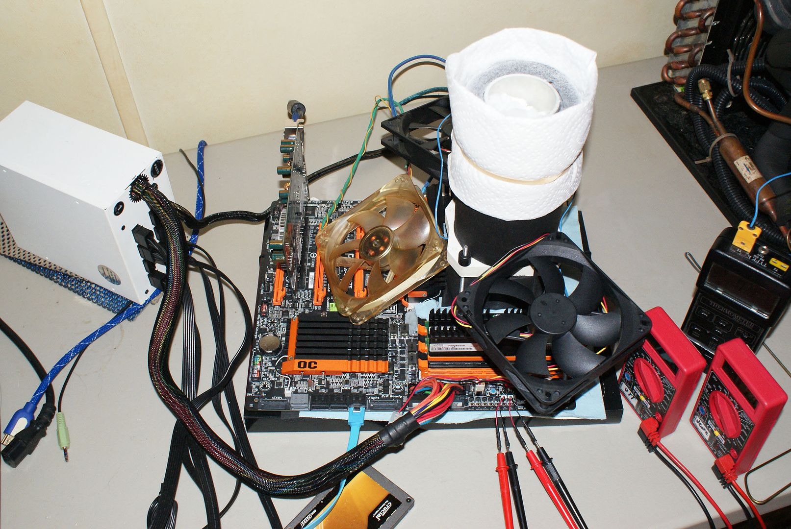
Custom built Dice / Ln2 Cooling pot by BartX @ OCN
Custom built Phase Change Cooler by SDumper @ XS / OCN
The following benchmarks were run three times on each board, at the same frequency and voltage settings, except where either board may have needed a voltage change by a notch here or there depending on available voltage choices, or in the event that one board simply required a voltage increase due to having a different actual delivered output voltage. The OC board appeared to deliver higher actual voltages than the UD7, so many times the UD7 would need voltages set higher to compensate for the lower delivered voltage. Actual voltages were not measured on the UD7, so any needed voltage increase based on loss of stability at a given setting would be based on my own personal thoughts and/or software readings of load voltages. Generally, voltages remained set the same across both boards in most all of the tests performed, a change, if any, would simply be minor compensation for the way the two boards deliver voltages and/or the differences in voltage drops or droops at a given setting.
After each set of tests was run, I took the highest and lowest results and tossed them out, using only the median result for each board on each of the benchmarks run for the comparison. The boards are so close to each other in these regards, any differences in performance outcome would only be due to minor BIOS or power delivery differences. The benchmark results were all very close, so choosing that result based on this methodology seemed to be a logical choice due to the very minor differences observed. There was no major differences in any benchmark, and the highest and lowest of each for either board was VERY close to the mid result as well, so the scores used below fairly and accurately represent each motherboard model, and their differences in respect to benchmarking are minor - if at all.
Programs used for comparison:
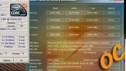
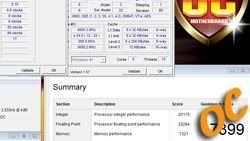
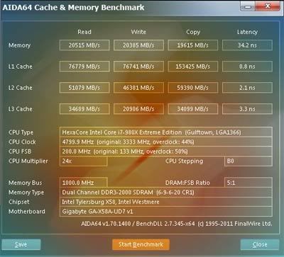
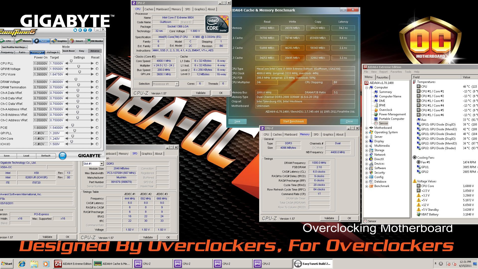
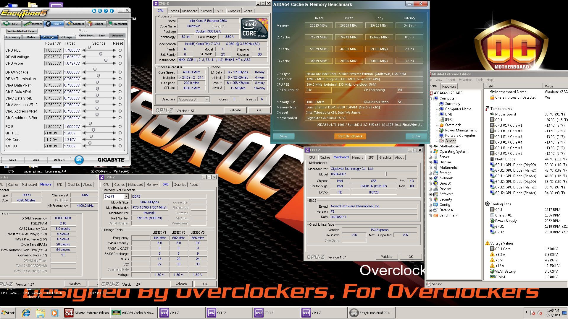
AIDA64 v1.70.1400
Previously known as Everest Ultimate, this is a great quick benchmarking and system information program - everyone should have a copy. It is not so much a hard testing tool for our purposes, but it does provide multiple stability tests, various bandwidth tests, and in-depth system hardware information. For this review it will be used to provide simple bandwidth and latency test results on each board.
AIDA64 | PC Benchmark | System Diagnostics | Network Inventory
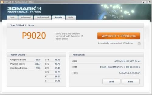
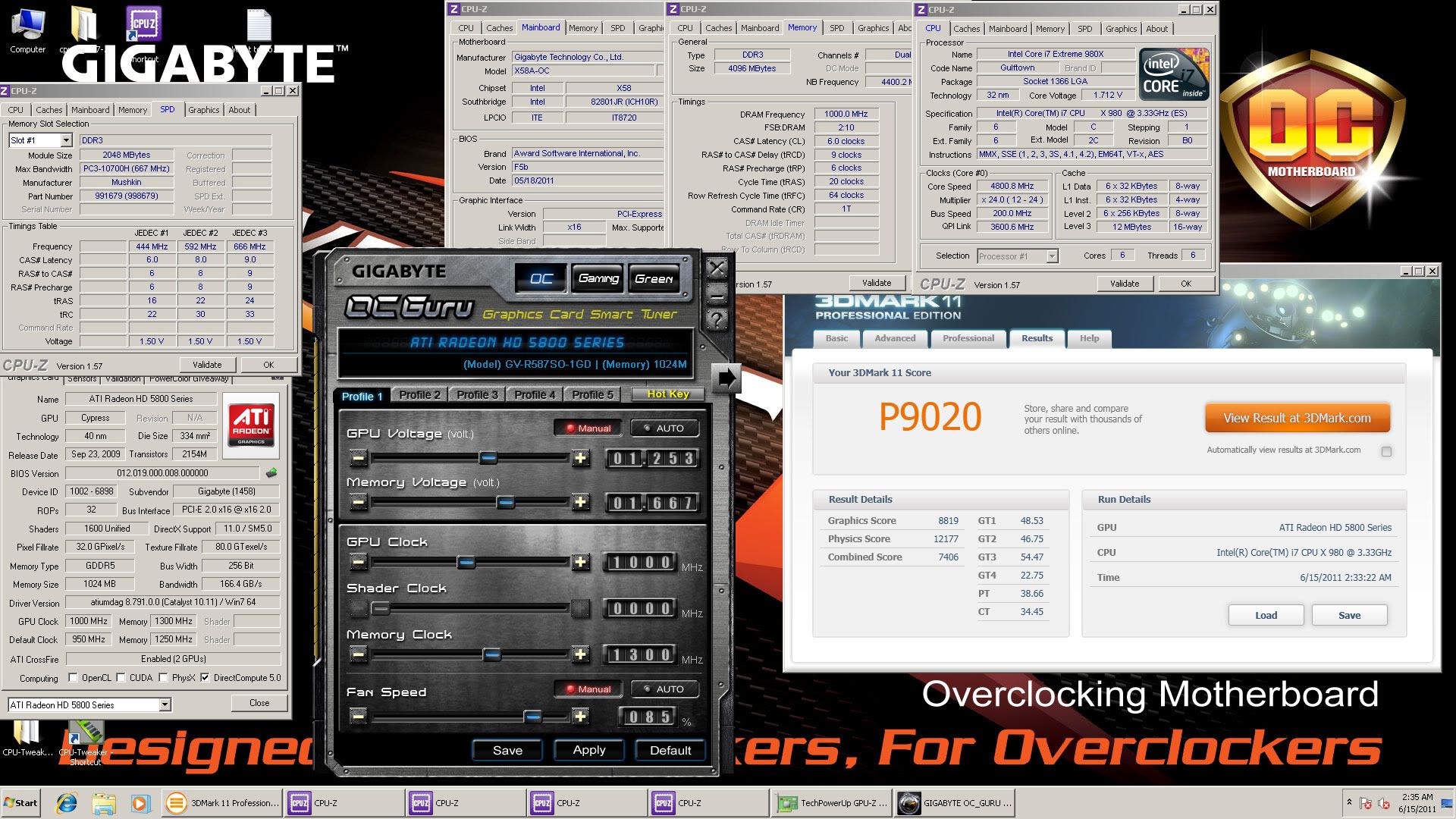
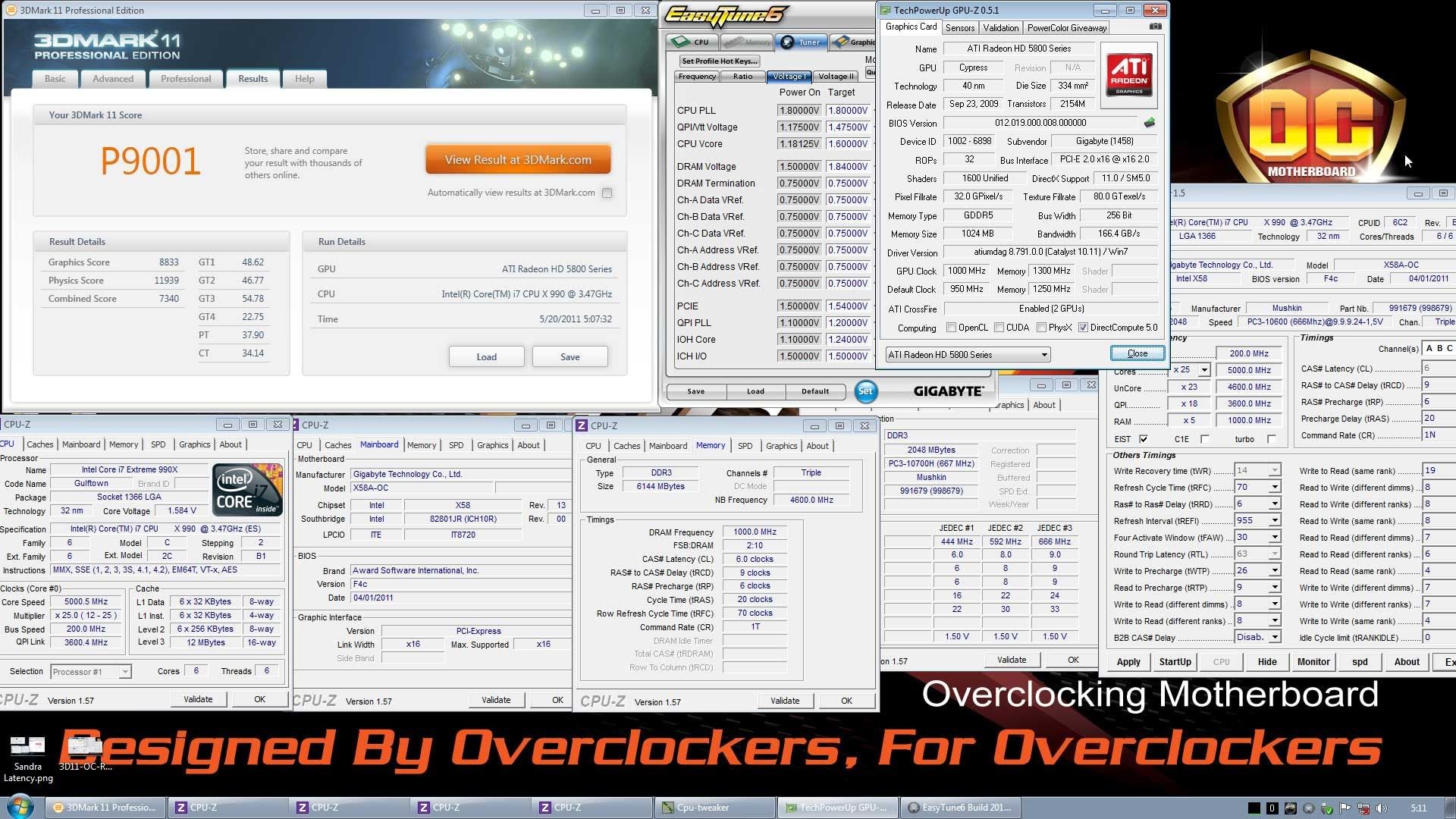
Futuremark 3DMark 11 Professional v. 1.0.1
Futuremark - Benchmarks - 3DMark 11
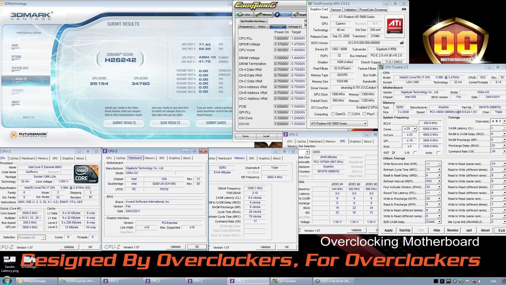
Futuremark 3DMark Vantage Professional v. 1.0.1
Futuremark - Benchmarks - 3DMark Vantage - Download
Geekbench V. 2.1.11 x86
Primatelabs - Geekbench
Hexus PiFast version 4.1 (Batch)
http://pifast.hexus.net/pifast.php
For more information also see here, and here.
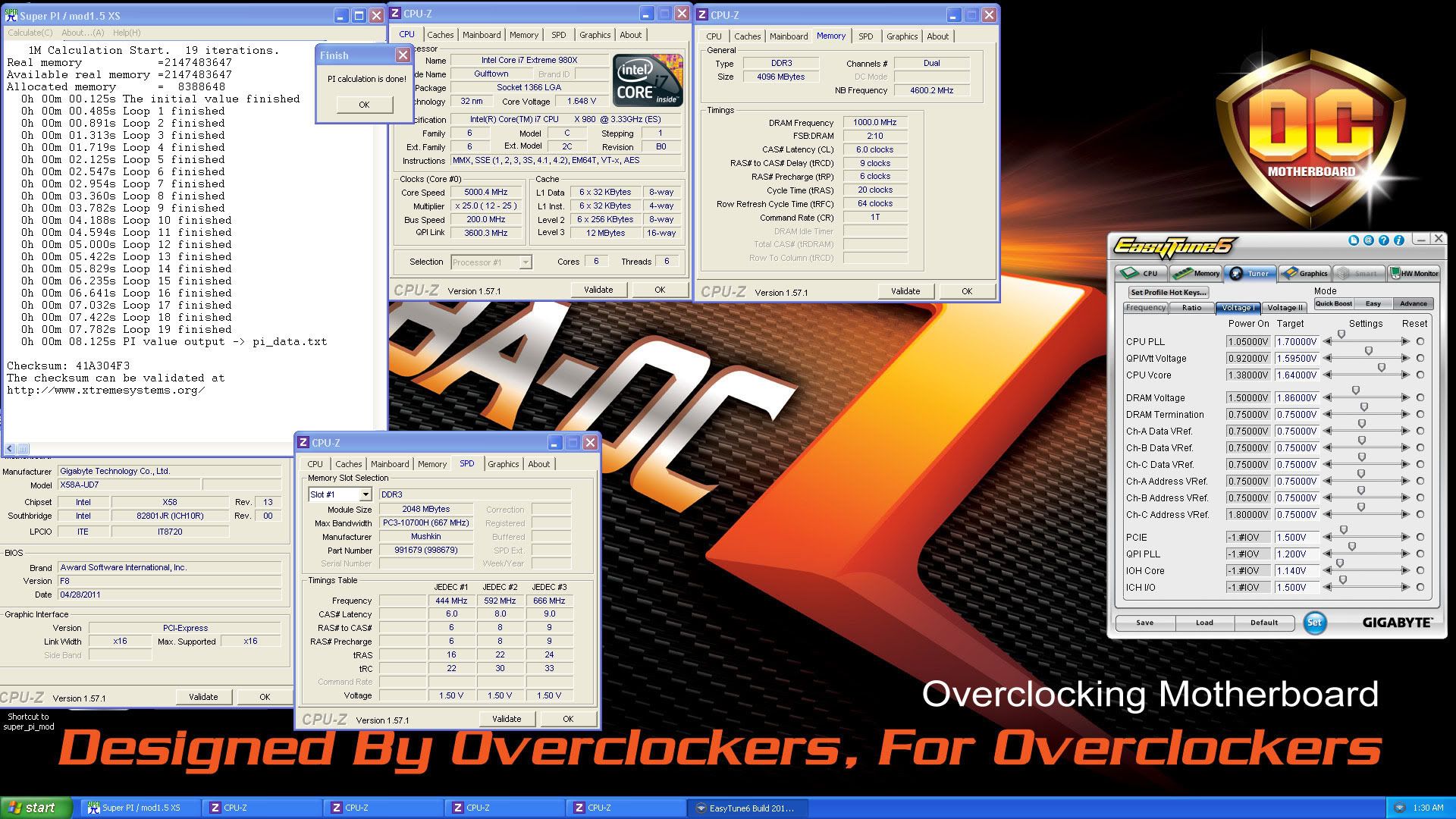
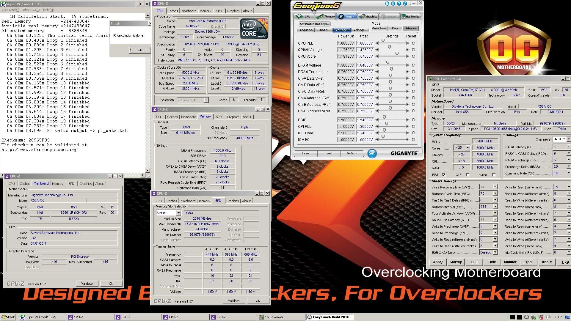
Super PI Mod XS 1.5V
SuperPI is a quick reference benchmark test often used when overclocking or comparing different hardware configurations.
Wikipedia - Super PI
Super PI Mod XS 1.5 Download - Techpowerup
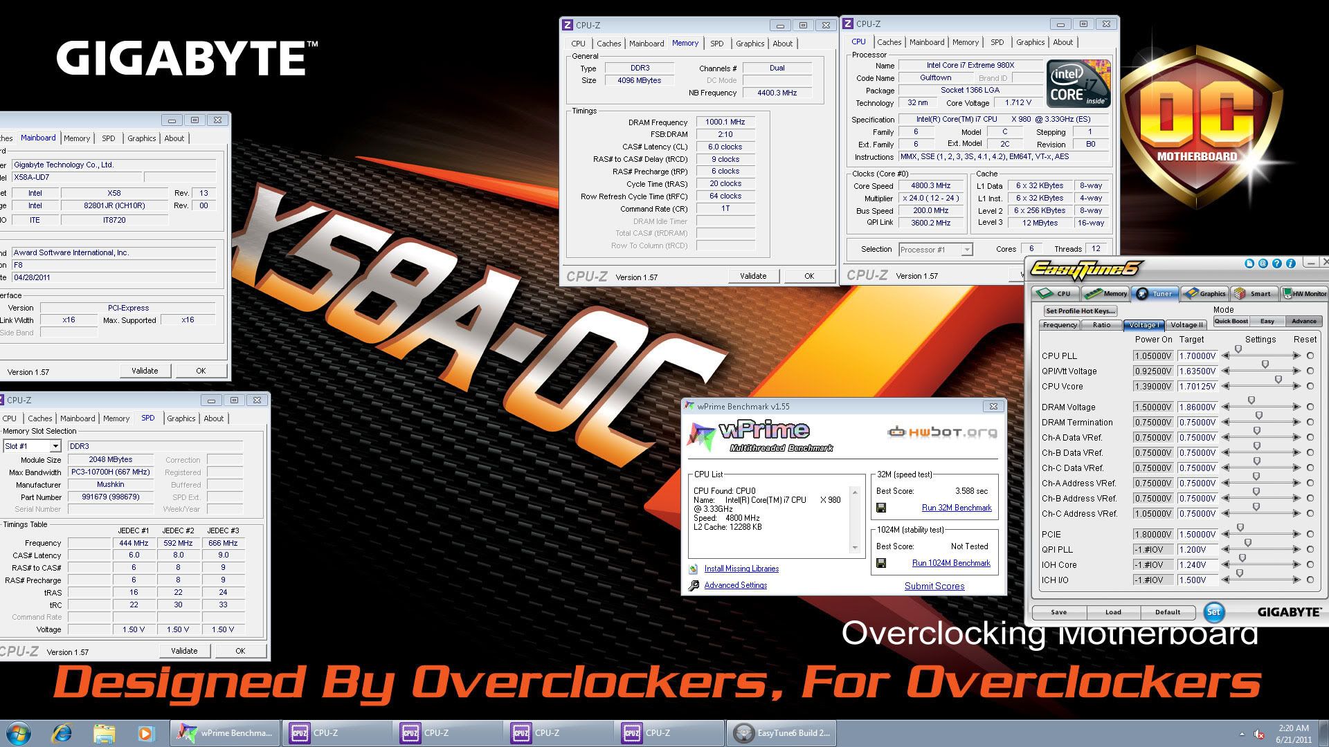
wPrime V. 1.55
wPrime Download - wPrime.net
AS SSD Benchmark V. 1.5.3784.37609
AS SSD benchmark is the latest and most commonly accepted SSD testing program, it determines the performance of solid state drives (SSD) based on many factors. The tool contains five synthetic as well as three practical copy tests (ISO, Program, Games).
AS SSD Solid State Disk Benchmark Download - Alex-is DOT de
ATTO V. 2.34
ATTO has been a major disk testing utility for many users, for quite some time, offering the ability to test performance using various transfer sizes and test lengths for reads and writes. It also offers several options to customize your benchmark testing including queue depth, overlapped I/O, a comparison mode and the option to run the test continuously.
This benchmark will be used to test 6GB/s SSD performance on the new Marvell 9182 controller on the OC motherboard, and the older 9128 controller found on the UD7.
ATTO Disk Benchmark Download - ATTOtech.com
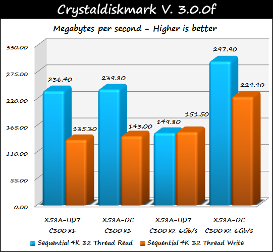
CrystalDiskMark V. 3.0.0f
CrystalDiskMark is another staple in the disk benchmarking world, offering measurement of sequential read and writes speeds, random 512KB, 4KB, 4KB (Queue Depth=32). Users may also select the method of how data is tested, random, 0Fill, or 1Fill - in the testing done for this review only the default testing method was used - Random Data.
This benchmark will be used to test SSD performance.
CrystalDiskMark Download - Crystalmark.com
Benchmark Comparison Results - OC VS. UD7:
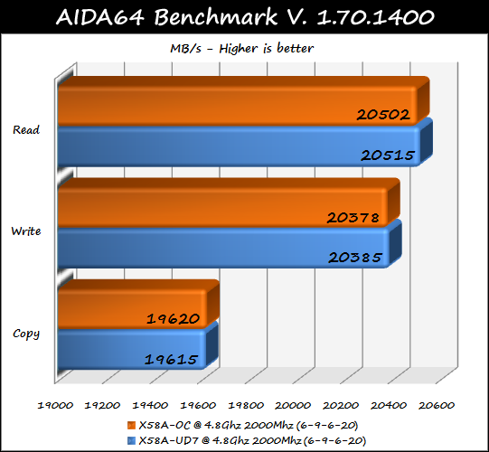
AIDA64 v1.70.1400
Not much to mention here, as you can see both boards scored almost exactly the same, meaning any minor difference was likely due to Windows services polling the CPU at different times.
The latency scores were exactly the same, so they are not graphed.
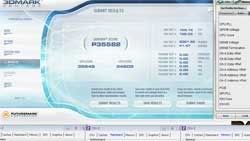
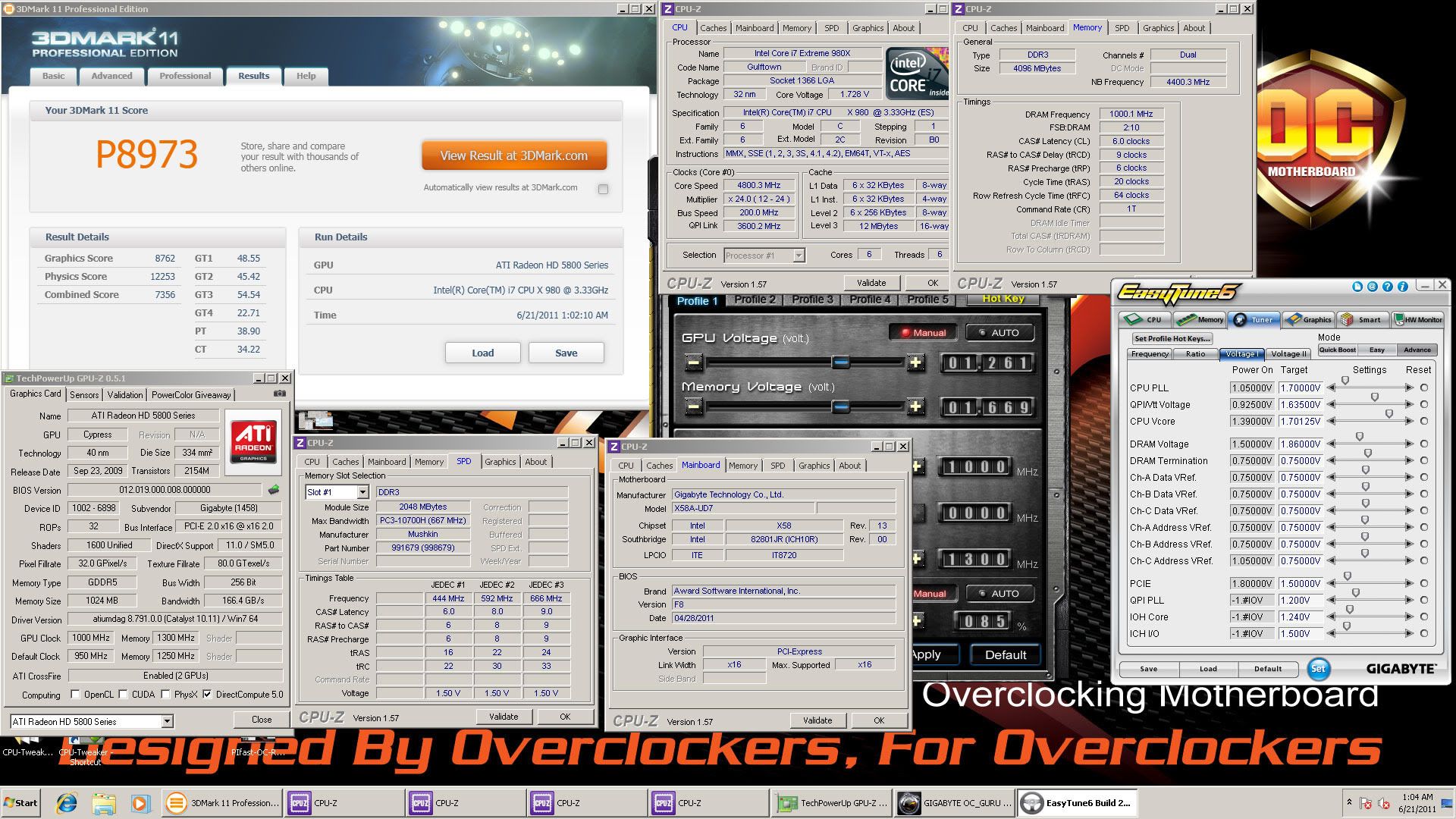
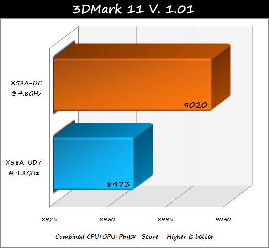
Futuremark 3DMark 11 Professional v. 1.0.1
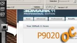
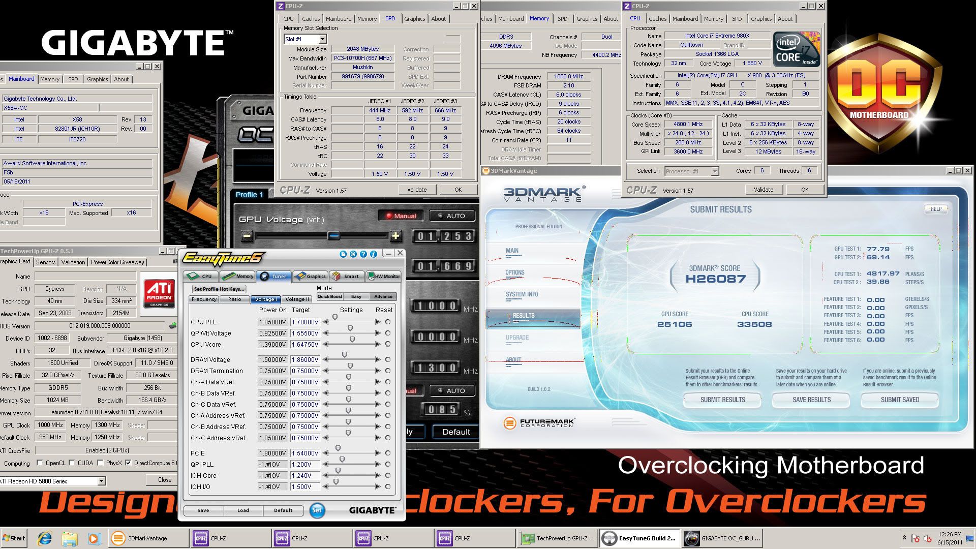
Here the X58A-OC comes out ahead by less than 50 points in 3DMark 11, as I mentioned above, scores were always very close - as seen many of the results.
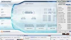
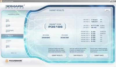
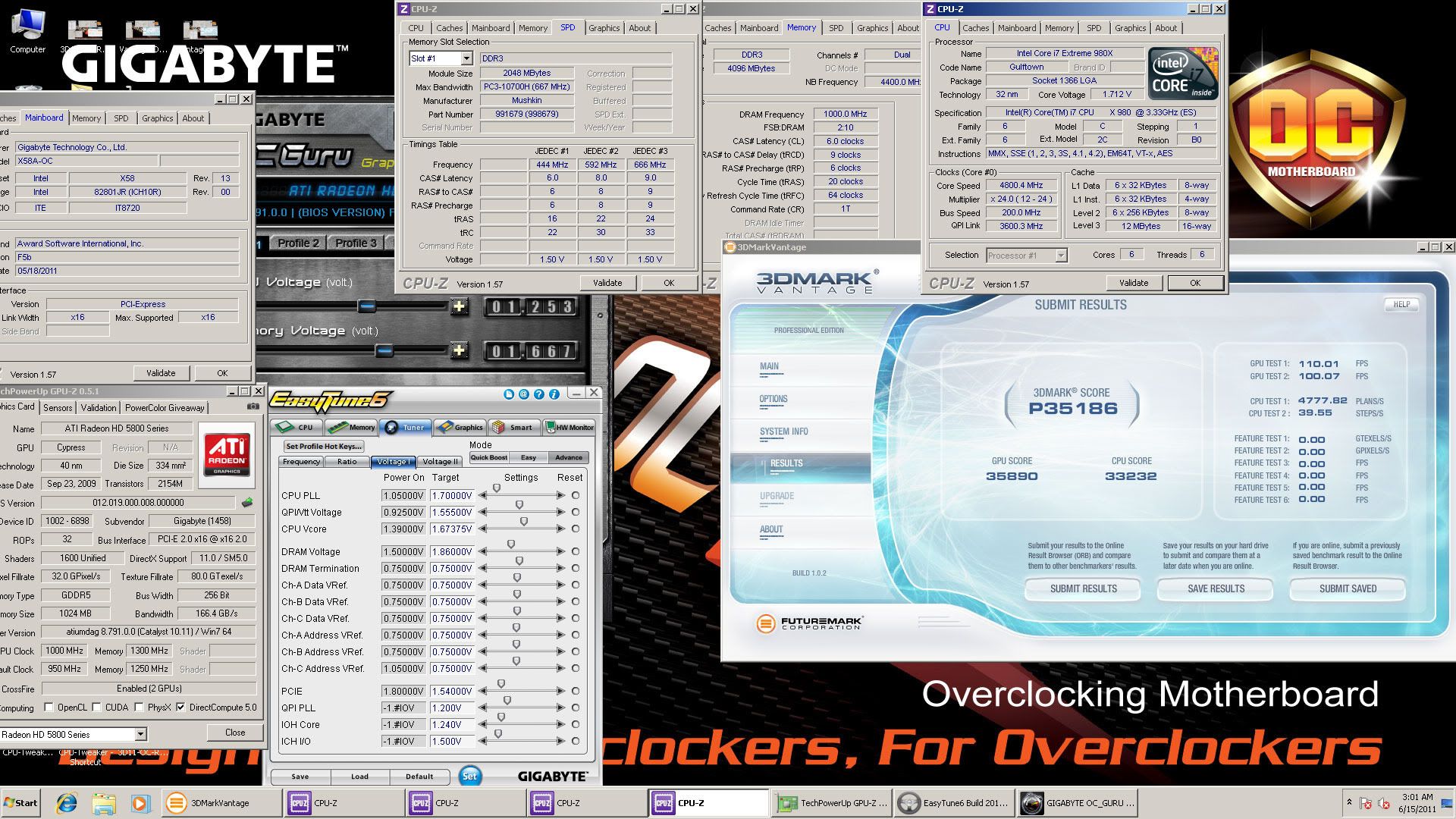
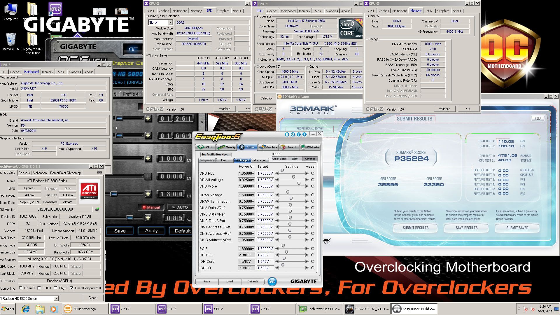
Futuremark 3DMark Vantage Professional v. 1.0.1
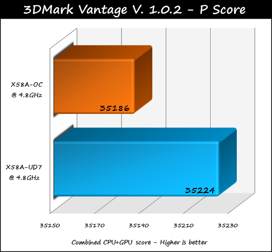
"Performance Setting Results "P"
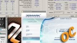
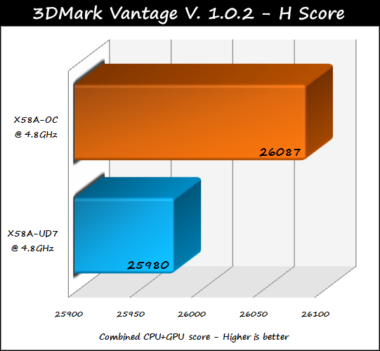
High Setting Results "H"
The UD7 came out ahead each time in my tests for the Performance score of Vantage, but each time it was by less than 50 points, leading me to believe this is likely due to minor BIOS differences between the two boards.
The OC board won each time during my testing for the High setting of 3DMark Vantage, but each time the win was by less than 120 points, again leading me to believe the differences in these scores are due to minor BIOS variances.
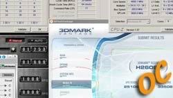
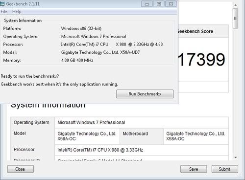
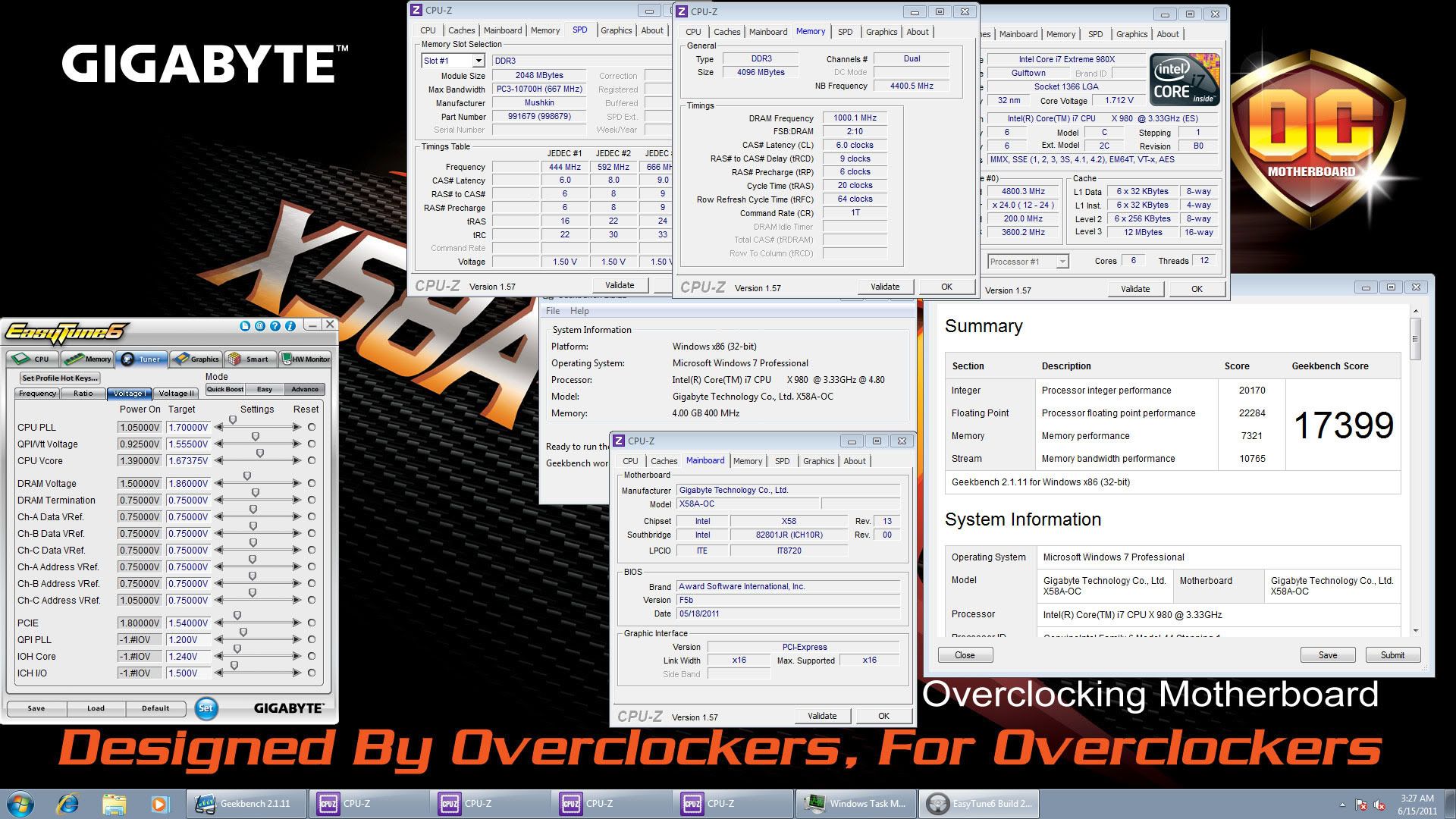
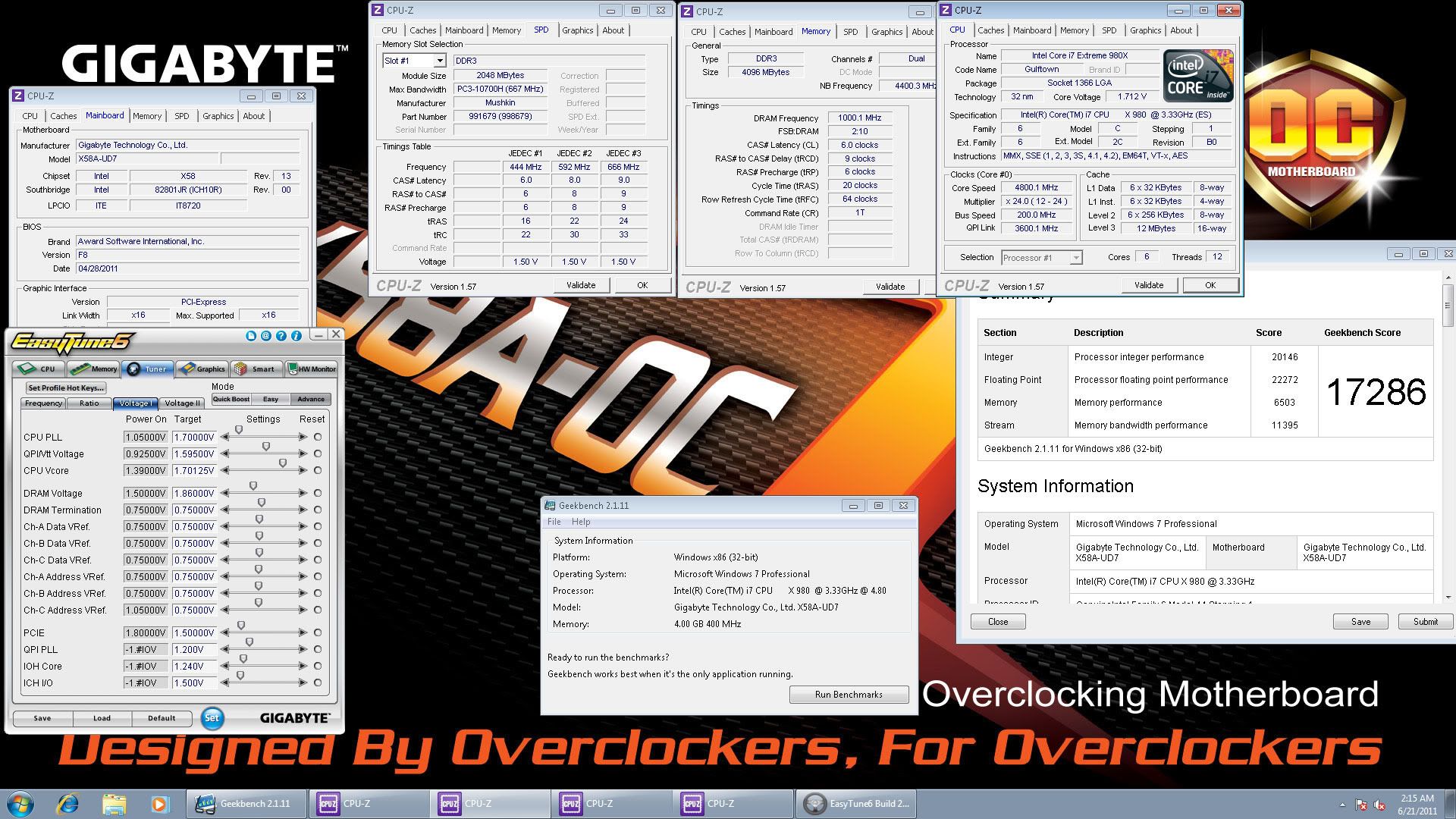
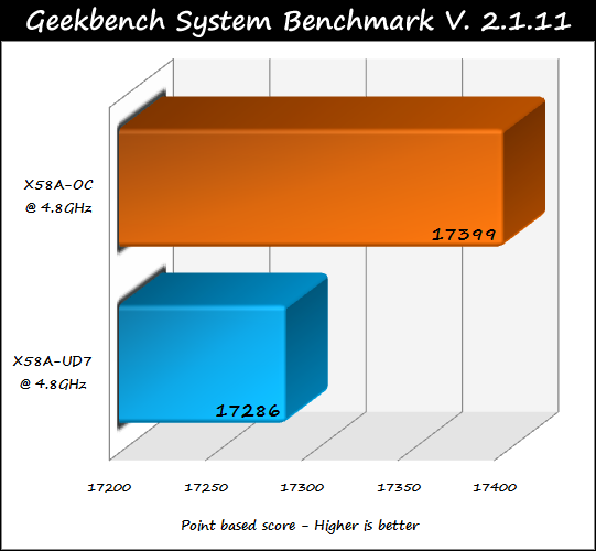
Geekbench V. 2.1.11 x86
The OC board comes out on top in Geekbench, each time leading by at least 100 points.
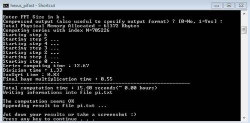
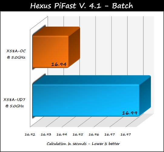
Hexus PiFast version 4.1 (Batch)
With the PiFast benchmark, the OC board leads the way during each round of tests, but each time it was by less than .12 seconds.
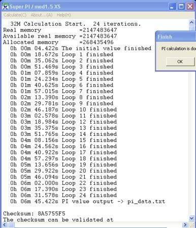
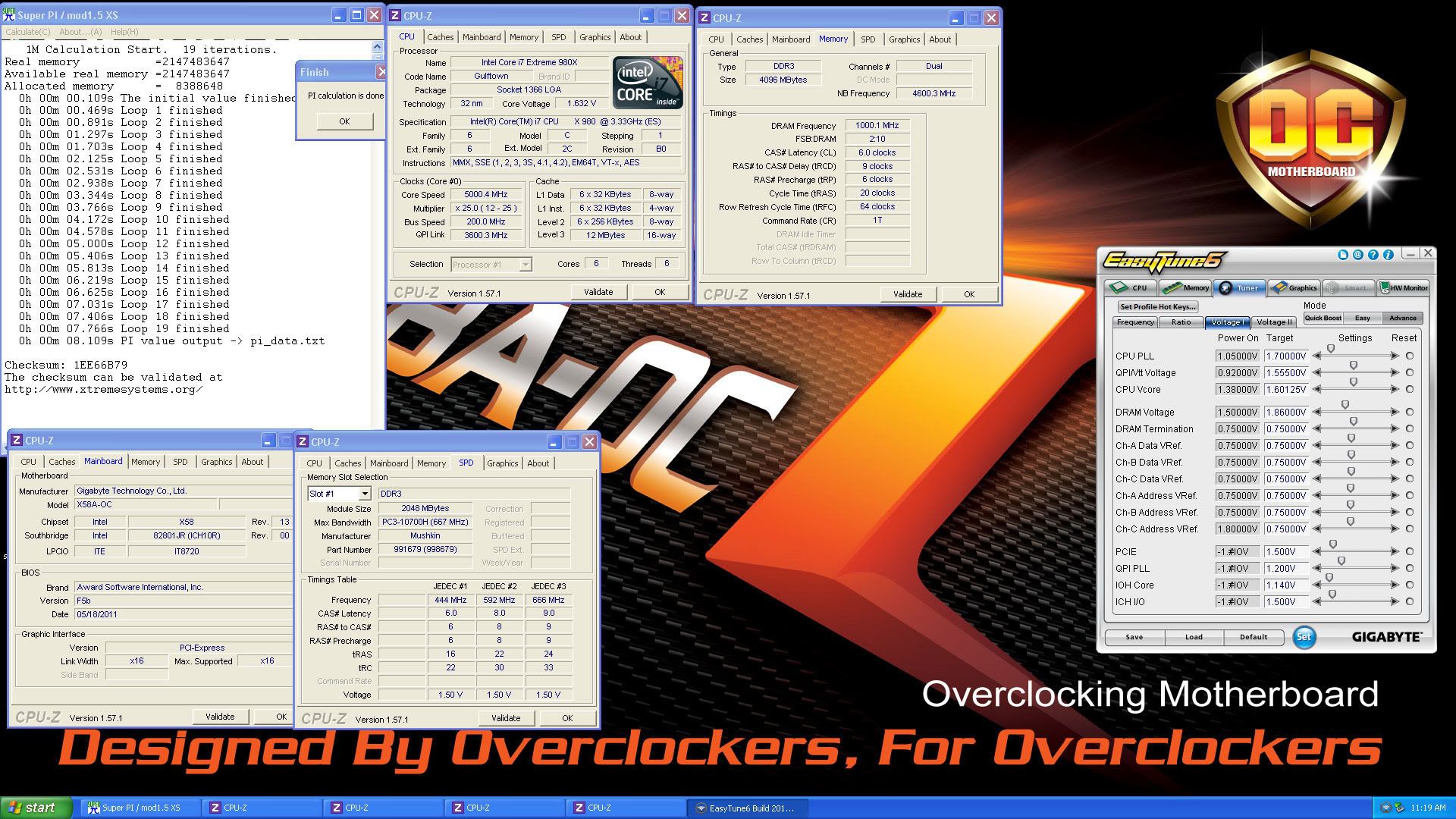
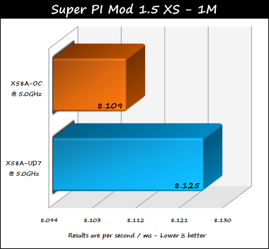
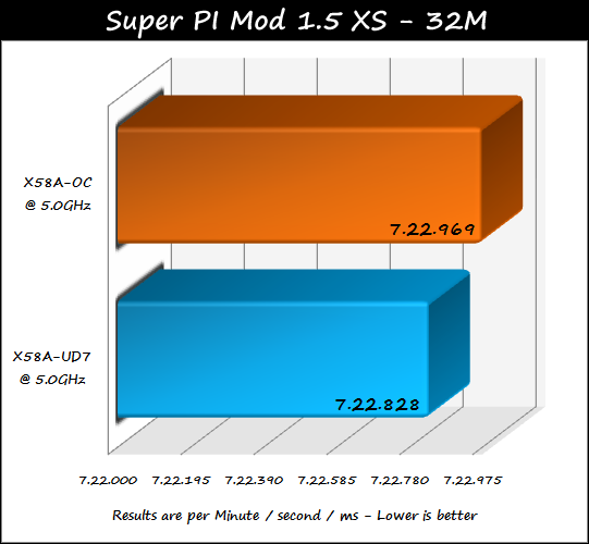
Super PI Mod XS 1.5V
1M Results
32M Results
The X58A-OC comes out on top in SuperPI 1M, this was the case each time I tested - but only by a fraction of a second..
The UD7 won each round of tests for SuperPI 32M, but each time it was only by less than .200ms, again, all likely due to minor BIOS differences between the two BIOSes.
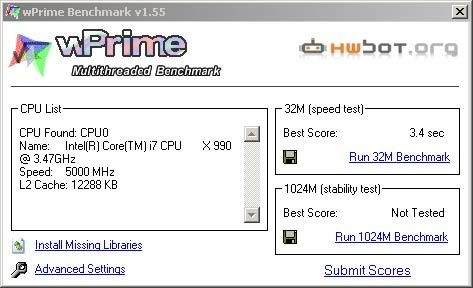
wPrime V. 1.55
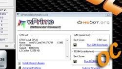
The OC board came out on top of each round of wPrime tests, by an average of .30-.50ms, again this is probably due to BIOS variances.
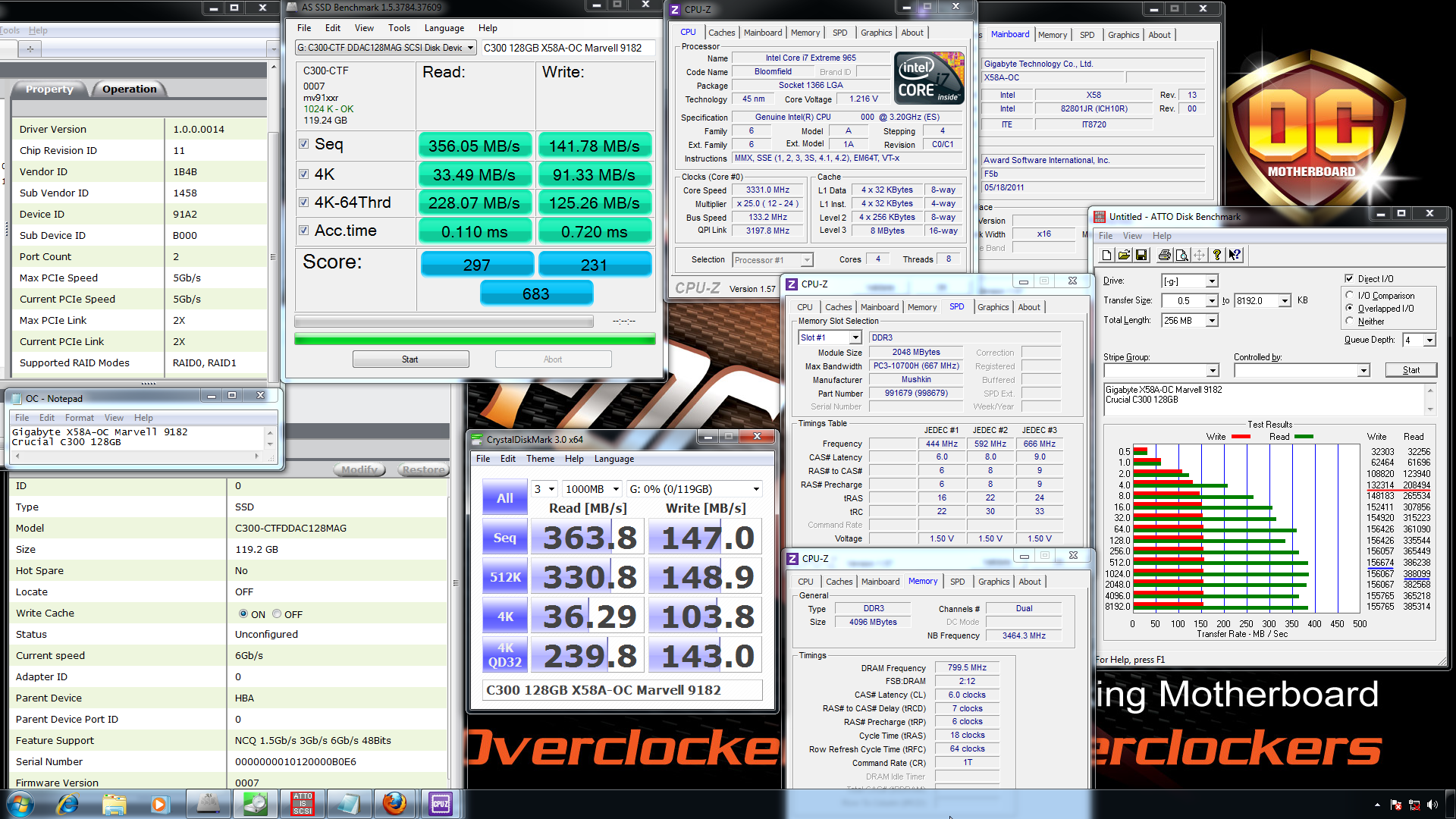
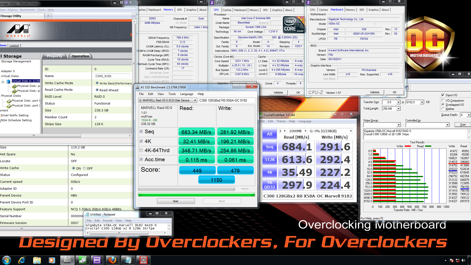
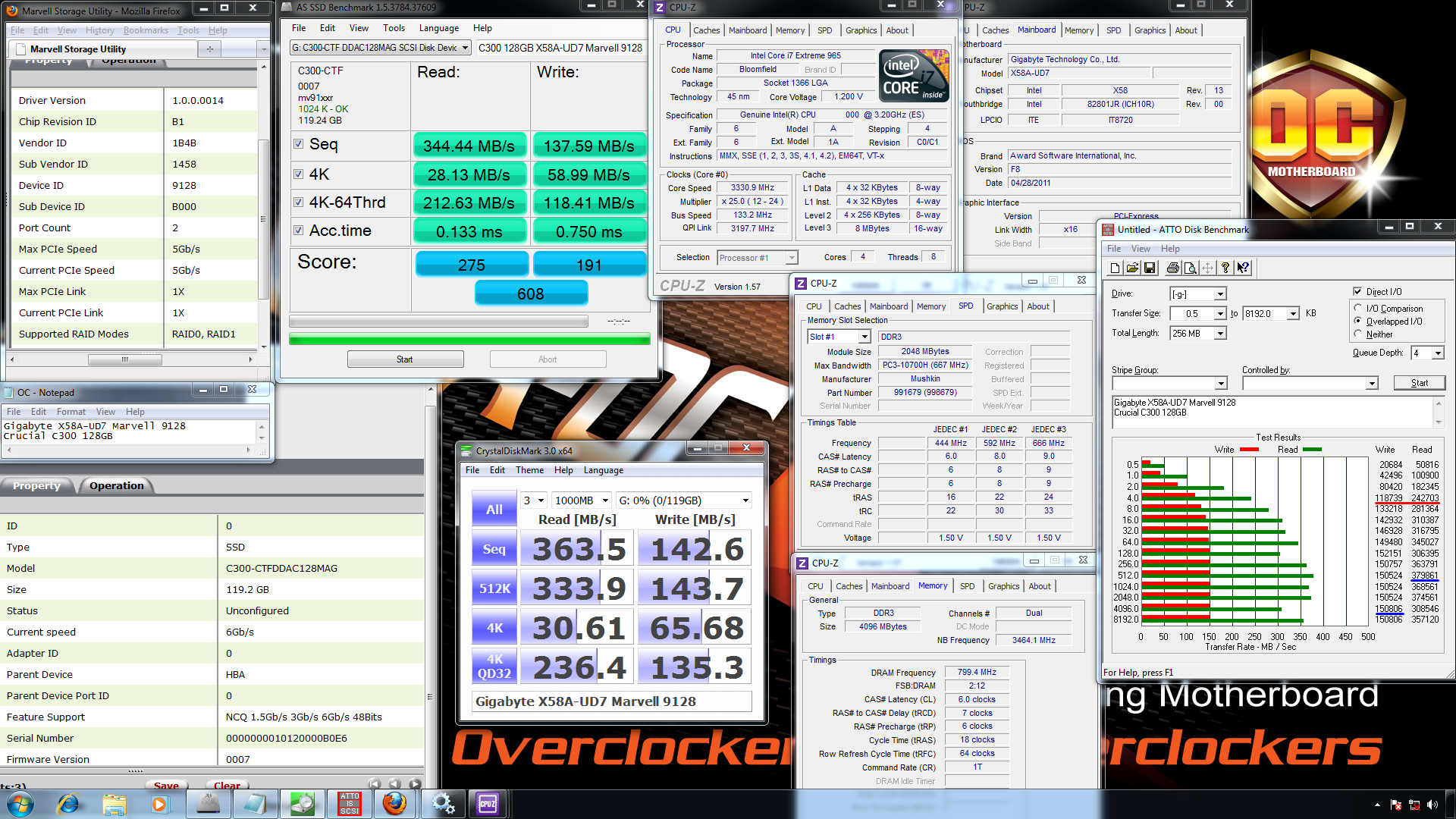
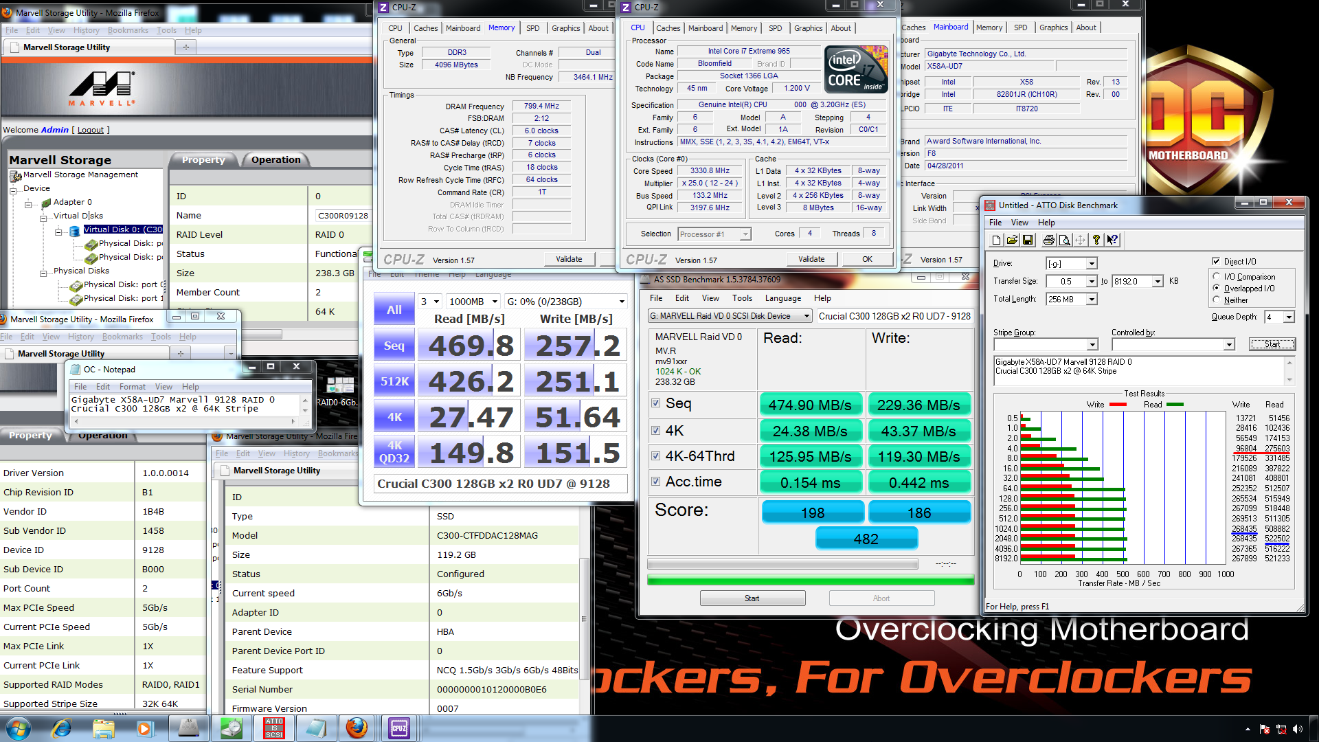
SSD 6Gb/s Testing Results - Marvell 9182 (OC) Vs. 9128 (UD7):
The new Marvell 9182 controller is vastly superior to the older, limited Marvell 9128 controller. The new 9182 utilizes dual PCIE lanes (x2) in comparison to the 9128 that only uses a single PCIE (x1) lane to transfer data. The 9182 is hardware based, and has it's own BIOS that is separate from the main boards BIOS, and it's BIOS offers more options than the older controller. The only drawback to this hardware based controller is that it must load the BIOS during POST like any other controller card, which can lead to some issues. At the time of writing this review the only issue I ran into that causes me to mention this is the fact that you cannot enable both the Marvell and Intel RAID at the same time. You can still use them both at once, but the Marvell control ROM is unable to load during POST, so you must build your array either before loading windows, or within windows using the Marvell web-based utility, which you would also need to manage the Marvell if you needed to make any changes (once both controllers are enabled).
X58A-OC Benchmarks - 9182
X58A-UD7 Benchmarks - 9128
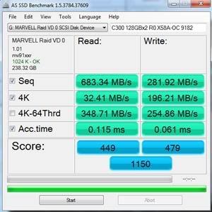
AS SSD V. 1.5.3784.37609
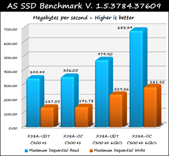
Sequential Maximum Read/Write
As you can see here, the 9182 controller on the OC motherboard is vastly superior at RAID in comparison to the 9182 controller on the UD7 motherboard. When it comes to using a single disk they are closer in performance, with the 9182 only leading by a small margin, at least for sequential read/write speeds.
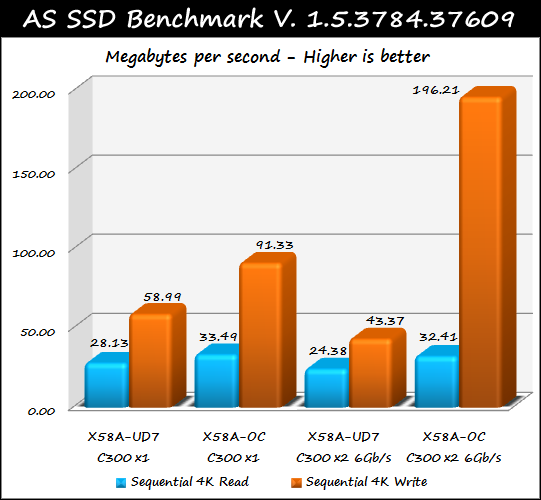
4K Maximum Read/Write
In the area of 4K file transfers, you can see how the new 9182 controller begins to show it's superiority.
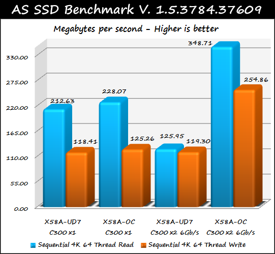
4K-64Threaded Maximum Read/Write
When using a single disk, heavily threaded performance with either controller is very close, much like the sequential results. In RAID there is no comparison, the dual PCIE lanes and the larger 128K stripe size supplied by the 9182 controller on the OC board makes it an obvious leader in performance.
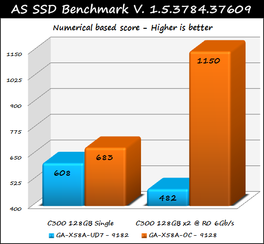
Overall Total Score
Again, single disk performance overall is fairly close for the two controllers, but in RAID the UD7's 9128 controller is no match for the OC's 9182 controller. To be fair, it is well known that the Marvell 9128 controller simply cannot handle SSD RAID arrays, I only included RAID on that controller as a part of this comparison to reiterate this fact and to show this in a graphical manner to you, my readers, and fellow overclockers.
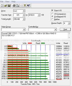
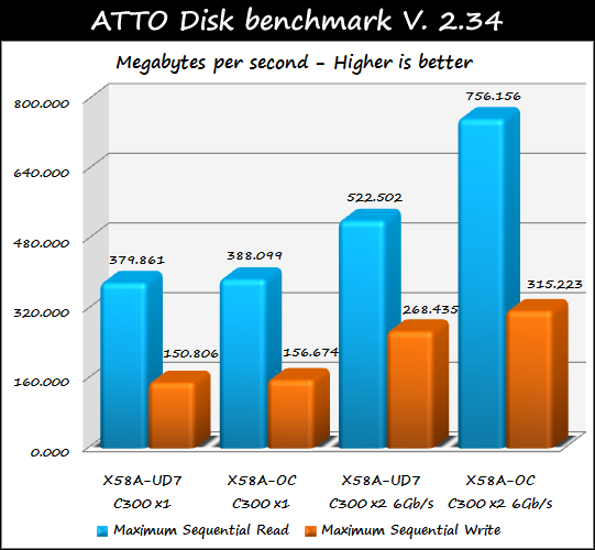
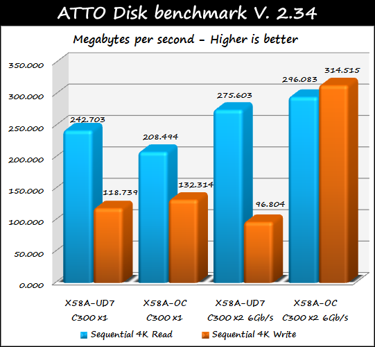
ATTO V. 2.34
Sequential Maximum Read/Write
As seen in the AS SSD tests, sequential speeds by a single disk on either controller are very much on par with each other. When in RAID, the choice of which controller is the prevailing leader is easy to see.
4K Maximum Read/Write
In this 4K round a single disk on the 9128 controller is faster at read speeds by a fair amount, but the 9182 steps ahead in write speeds.. In RAID mode the 4K reads vary only a small amount on the OC board vs. the UD7, but the writes are more than 4 times faster on the OC compared to the slower speeds of the UD7's 9128 controller.
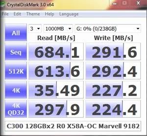
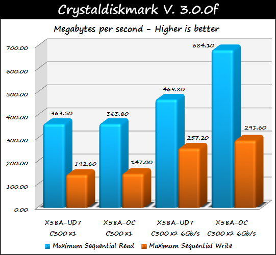
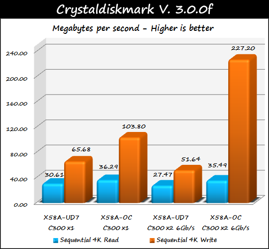
CrystalDiskMark V. 3.0.0f
Sequential Maximum Read/Write
Again, single disk performance on either controller is very close when it comes to sequential read/write speeds, but the RAID performance of the 9182 is without a doubt, considerably the better performer.
4K Maximum Read/Write
The 9182 controller on the OC board comes out on top of all tests here, but again with a single disk the difference is not as large as it is in other areas.
4K Que Depth 32 Maximum Read/Write
Single disk tests on both controllers are very close here at the transfer size of 4K at 32 que depth sizes. RAID Performance, however, is noticeably improved on the 9182 controller that is utilized on the X58A-OC motherboard.
990X Testing Results (Originally Intended for comparison with the UD7)
My intentions were to use these results for the UD7 comparison, however, the 990X CPU was damaged while testing on the OC board, so I was not able to complete my comparisons on the UD7. The 990X lasted through many other higher benchmarks before these, and was fine afterwards for several days as well, it ended up loosing three cores while idling at 5GHz while I was gathering some of the following results. Due to this issue, I had to go back and re-do all my testing again on both boards using my 980XSo, I decided to include these results as well for anyone interested. These are the same benchmarks as tested above except all at 5GHz with 990X, minus AIDA64 and Geekbench as I hadn't decided to include those until later in my testing.
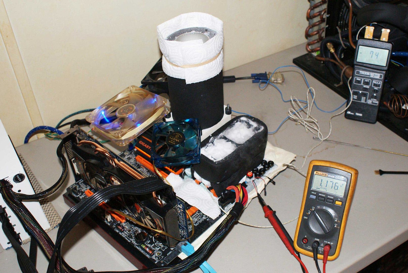
Random Extreme Overclocking Results:
Once this board is frozen you may run into an issue with the Clear CMOS and PWM switches. This is something I noticed looked a little too close for comfort when images first started appearing online before the board launched, and I thought these would possibly be relocated before the final version was set in stone, but as you can see they have not.
So, when freezing this board you must either set these and forget them under your insulation, or you could possibly drown them in Vaseline or dielectric grease. Dry ice is as extreme cold as it gets for me, and when the board is at -74C these are frozen SOLID fairly quick, insulated or not. Under phase cooling (-40-50C) they are fine, but if you are using dry ice or Liquid Nitrogen (LN2) that would be much colder (-196C), you will need to decide what you want to do before the freezing commences.
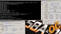
Maximum Bclk Results & The Bclk World Record!!
*** World Record Bclk for X58 / 1366 Secured with X58A-OC!!! ***
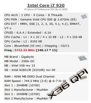
Shortly before obtaining the world record for X58 Bclk, I was able to secure third place global with 269.28 Bclk, which was first place for the X58A-OC motherboard. This was done using phase cooling, and I wrote a news article about that session that you may view here @ TweakTown.
Being so excited about getting third place, I had to plan a dry ice session soon, and it was only a few days later the first place record was mine, thanks to the incredible X58A-OC motherboard! Being so excited to hold a first place global record, I quickly made out a news article on that as well which you may view here @ TweakTown.com. The link contains images of the setup used, and other clocks and benchmarks obtained during the same session as well.
Please click on any CPU-z image below to view validations
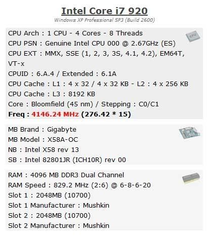
Lsdmeasap's 920 276.42 Bclk Submission @ Hwbot
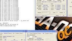
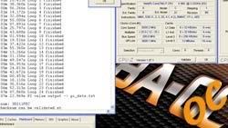
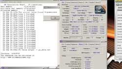
Here is a video I made that same day showing my bootup at 260 Bclk, and then taking the system up to 276 Bclk within Windows. This was taken with a cheap low resolution camera, so please pay no attention to the quality.
http://www.youtube.com/watch?v=ojrkUdnNQg4
Here are the Top 20 current HWBot standings for X58 Reference Clock, you may also click the link below and see an updated search of the HWBot records to see if anyone has submitted a higher Bclk yet.
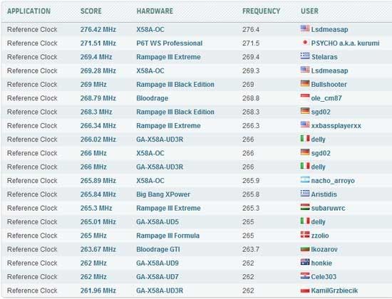
Top 20 current HWBot standings for X58 Reference Clock (Bclk)
As you can tell, pushing for highest Bclk is something I really like to do. Everyone has their own "cup of tea" so to speak, and Bclk is one thing I really enjoy when it comes to X58 benching. It's not an easy thing to do, it takes a lot of skills, patience, and of course, the right motherboard and processor. Reaching a very high Bclk is a "Luck of the draw" sort of thing and is dependent on the processor, once you have the right motherboard, some CPU's can do very high Bclks while others struggle to keep up with the rest. As you can see below, with all of the CPU's I have reaching 250 or above, only one is well above the others! And I almost didn't test Bclk with that CPU too, but I'm glad I eventually did. Why I almost didn't test it is because it's an early sample with locked memory multipliers (8/10), and it's never really done anything impressive - until now.
Other notable 920 Bclk's
965 Bclk
W3520 Bclk (Phase only)
980X Bclk
990X Bclk (Phase only)
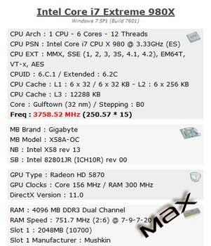
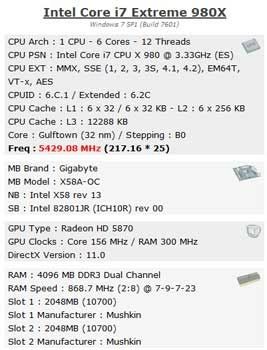
Maximum Overall CPU Frequency:
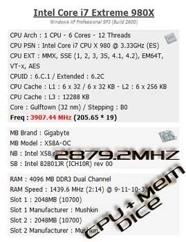
5.429GHz - 980X
Lsdmeasap's 980X 5.429GHz Submission @ Hwbot
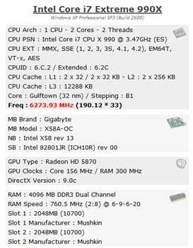
6.273GHz - 990X
Lsdmeasap's 990X 6.273GHz Submission @ Hwbot
Maximum Memory Frequency:
Ridgeback 998826 Left (Air) - Radioactive 998966 Right (Dice)
Various Super PI 1m & 32M (+1 PiFast)
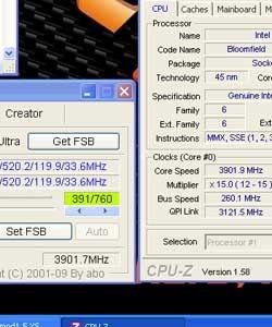
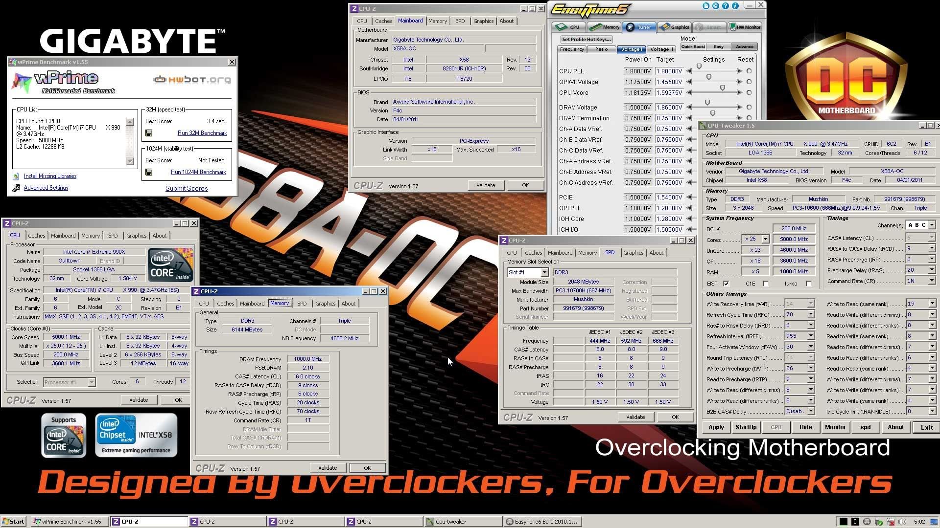
272.5 Bclk Super PI 1M
250-265 Bclk Super PI 1M
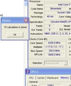
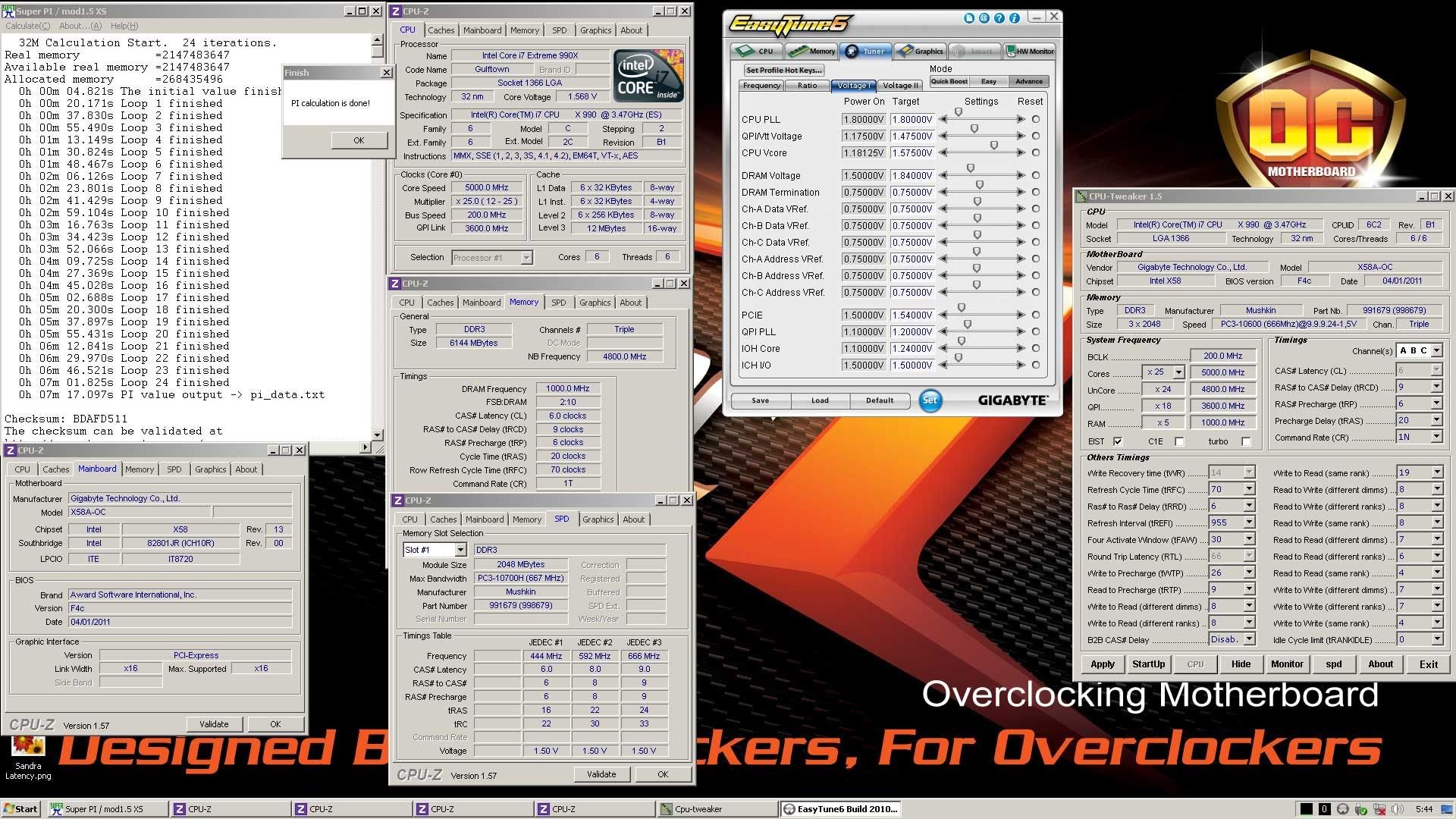
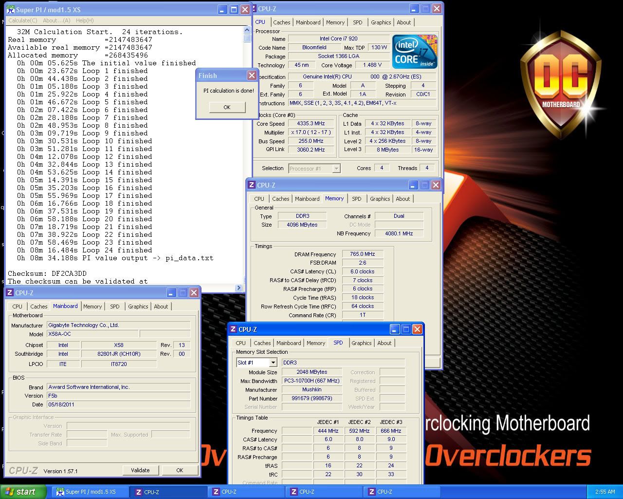
6 minutes 45.422s Super PI 32m @ 5.5GHz (Personal X58 best)
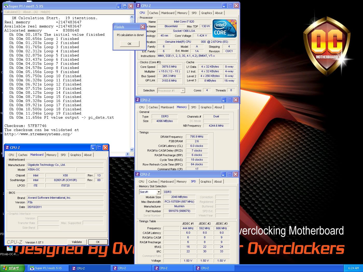
7.296s Super PI 1m @ 5.56GHz (Personal X58 best)
15.40 seconds PiFast @ 5.5GHz (Personal X58 best)
Final Thoughts & Conclusion:
I'd like to start off this section with an apology to my readers!
I am sorry it has taken me such a long time to get a review out on this awesome motherboard!!
Putting together a review in itself is not an easy task at all. Having to take the time to learn the board's unique abilities and have the opportunity to properly test and benchmark, isn't something I could do on a daily basis, and it is not a simple task. Using my phase cooling setup was ideal to test any time, but in order to do some of the actual overclock benchmarking that this board deserves to see, I had to find the time to squeeze into my tight schedule when to setup extreme overclocking sessions (Dry Ice) and then spend the time benching for those periods. On top of that, I had a processor fiasco midway through my data collection that prolonged my testing, making me start all over with a different processor. So in the end, it ended up taking me much longer than I had planned to have this review ready for you all to read, and for that I apologize greatly!
I would have loved the opportunity to be able to get in a few more benching sessions before I finished this review, but I've been unable to find the time needed to do so quickly, and this review deserved to be published as soon as possible. I normally spend 8-10+ hours benching with dry ice, I simply don't have enough free time to bench with it more, in time to add to this review. The GA-X58A-OC motherboard has been nothing short of a dream to work with, and I have thoroughly enjoyed the times that I was able to spend benching under extreme conditions!
Throughout the time I've spent testing and overclocking on this board I haven't ran into any major unexpected issues, it's been unbelievably fun to bench with, and I eagerly look forward to using it each time I plan to bench as I never know what awesome score I'll see next. I hope that GIGABYTE continues the "OC" line of motherboards, and they have mentioned plans of future models, so hopefully that will remain true. The X58A-OC being their first release in this newly (Self) created motherboard category has been a great step forward, there are few things I'd like to see improved in future models (See cons), but all in all it's a very impressive motherboard and is a great move in the right direction for motherboard technology itself and overclockers alike.
Everyone in the overclock community has waited a long time to see this board released, some patiently, and some not so much (Myself included haha). GIGABYTE released images and information long before the actual release of the board, which made all of our waiting very difficult, but all of that is over now and the board is available to anyone that would still like to grab one while they are still on the market. Currently, here in the US, you can purchase your very own X58A-OC motherboard here at Newegg.com for $359 plus a $30 mail-in rebate. That may sound like a high price, but the quality of the motherboard you get for your hard earned money makes it well worth the cash spent. In contrast this board comes in at a price point that is $100 less than the GIGABYTE G1-Assassin gaming board, and only about $25 more than your average GA-X58A-UD7 price, so in reality GA-X58A-OC at $329 (minus rebate) is easily a great deal.
If you are looking for a great replacement to your aging 775, 1156, or even X58 board, the X58A-OC comes highly recommended by me! This board's design is a crowning achievement in motherboard technology, easily surpassing all other X58 boards with which I've had the opportunity to bench. The high quality components, new on-board overclock features, and easy to use BIOS, make this board reign supreme in the X58 world and I highly recommend grabbing a piece of motherboard history by purchasing one today!
PRO's +
1. Multiple on-board frequency buttons and switches - An overclocker's dream, and very easy to use!
2. On-board voltage readout points and connection headers - A very welcome addition!!
3. 8 on-board fan headers (7 of which are PWM & controllable) - This is great for daily use and overclocking as well to some extent
4. Multiple on-board temp sensors + ability to display very low negative temperatures
5. Very easy to insulate CPU and PCIE area for extreme overclocking sessions - Saves time!!
6. PCIE slot arrangement is perfect for larger dual and triple slot graphics cards
7. Highly improved Marvell 6GB/s controller (9182)
CON's -
1. Location of the Clear CMOS and PWM Switches - As seen above these freeze due to being too close to CPU socket when frozen, you must set before they freeze and Clear CMOS via battery / PSU if needed
2. Lack of any new "Overclocking" BIOS options - For an "OC" board I expected to see some new BIOS options directed specifically towards overclocking
3. On-board Debug POST LED placement - The LED is difficult to view from most any angle once the board is setup
I'd like to offer a huge thank you to everyone @ GIGABYTE & Mushkin for their continued support!!!
Big thanks to Crucial and NXZT for providing some of the hardware used in this review as well!
One can dream right? Right!!
I'll leave you with some of my hopes and dreams... until we meet again.
I am getting used to GIGABYTE's new black PCB's, and I really do like the X58A-OC board's current orange and black theme.
But I think an OC board done in light blue and black would have looked awesome as well!
Hopefully GIGABYTE will carry on the OC motherboard line, and deliver something similar to the images here in the future!!
Baby blue and black would be SO SEXY!
(Hint, hint @ GIGABYTE)
Disclaimer: This image, and the one directly above it, are NOT GIGABYTE products, and are NOT meant to be a depiction of any future GIGABYTE product!
These are images of the GA-X58A-OC motherboard that I Photoshopped to show what it would look like in a blue and black theme.


 Reply With Quote
 fantastic comparasion!


Bookmarks