


Sandy Bridge appear on the horizon this year for overclockers. Some of us managed to get decent results from the new silicon. But lots of fun still awaiting us in Q2 2011, when updated B3-stepping motherboard wave reach the market. I was honored to test ASUS and Gigabyte top motherboard in a first wave, with B2 stepped PCH's, and stressed both boards quite hard for whole January and February, but no major issues on both. I had UD7 running RAID 5 array of three WD1002FAEX drives without issues (2 disks on SATAIII ports, one on SATAII).
Rev. B2 boards are still good for overclocking and 24/7 use, and while you run SATA3 ports (two native PCH-powered on each board) - you are safe, as SATA3 port transceivers unaffected by "wear-out bug". If you want my opinion on this - problem is bit oversized. But I understand vendors politics, it's not good if user loosing it's data/storage by hardware bug. Ok, back to review side now.
ASUS ROG Maximus IV Extreme and Gigabyte P67A-UD7 for Intel Sandy Bridge
This report covers two flagship boards designed to run Sandy Bridge platform from enthusiast overclocker point of view. Overclocking here means pushing system to maximum performance possible, using all available tools and tricks, but also keeping stable and robust operation modes. Also there will be short analyze of hardware components used, their usability and overall experience. I decided to put some more light into engineering efforts put into P67 motherboards, rather than make lots of benchmarks and ton of useless numbers, which represent only few chosen configurations.
Configuration under tests:
Processors used:
Intel Core i7 2600K "Sandy Bridge" processor, LGA1155, ES D1 stepping.
Intel Core i7 920 "Nehalem" processor, LGA1366, Retail D0 stepping.
I've selected widely used i7 920 processor for already old but still high-end Intel platform, and latest Intel 2nd generation Core i7 with top SKU and unlocked multiplier, what is very attractive for overclockers. Unlike Intel hexacores, 2600K cost about three times less, and able to deliver very good results even on air-cooling.
Motherboards used:
ASUS Maximus IV Extreme for LGA 1155 platform, Intel P67 + NVIDIA NF200 bridge.
Gigabyte P67A-UD7 for LGA1155, Intel P67 + NVIDIA NF200 bridge.
ASUS P6T6 WS Revolution for LGA 1366 platform, Intel X58 + NVIDIA NF200 bridge.
As for motherboards selected - it's interesting how two high-end boards perform in various tests using same hardware setup. Workstation board with NF200 bridge was used for 1366 i7 chip.
Cooling used:
Skythe Yasya with stock fan + Nidec TA500DC 120x120x50mm 2.7A for cold air tests
Asetek Vapochill LS for subzero
For more real-world scenario I've just took random heatpipe-powered cooler with 120mm fan. Subzero cooling is reserved for extreme tests in upcoming extended article.
Memory used:
Kingston HyperX DDR3 memory 2x2GB for both platforms (KHX1600C8D3K2/4GX)
Corsair Dominator GT 2x2GB sticks
Videocards used:
NVIDIA GeForce GTX 480
NVIDIA GeForce 8600GT for motherboard VRM tests
Fermi-powered videocard used to test 3D performance of new platform. Old 8600GT installed for VRM and CPU tests, to keep noise pickup and EMI from high-power videocard away from actual motherboard VRM measurements.
Storage:
HDD 160GB Samsung SATA2
Simple 7200rpm drive for booting OS, test apps storage.
Power supply:
Enermax Revolution 85+ 1250W
Solid and powerful power supply with quiet rails, just to be sure nothing limits us here.
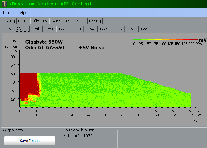
Gigabyte Odin GT 550W
PSU for ambient tests on ASUS board.
Software configuration
MS Windows XP 32-bit
MS Windows 2008 R2 64-bit
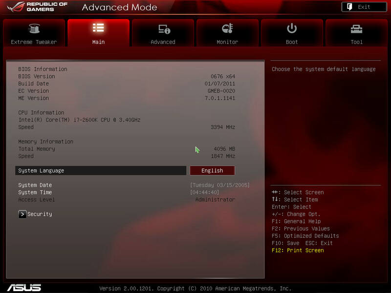
BIOS for ASUS board - 0676
BIOS for Gigabyte one - F7A from 2011/01/11
Let me tell few words about used equipment. I wanted to learn how to overclock new platform, and how to make it stable and fastest possible, and that is mission impossible without continuous monitoring and adjusting critical parameters.
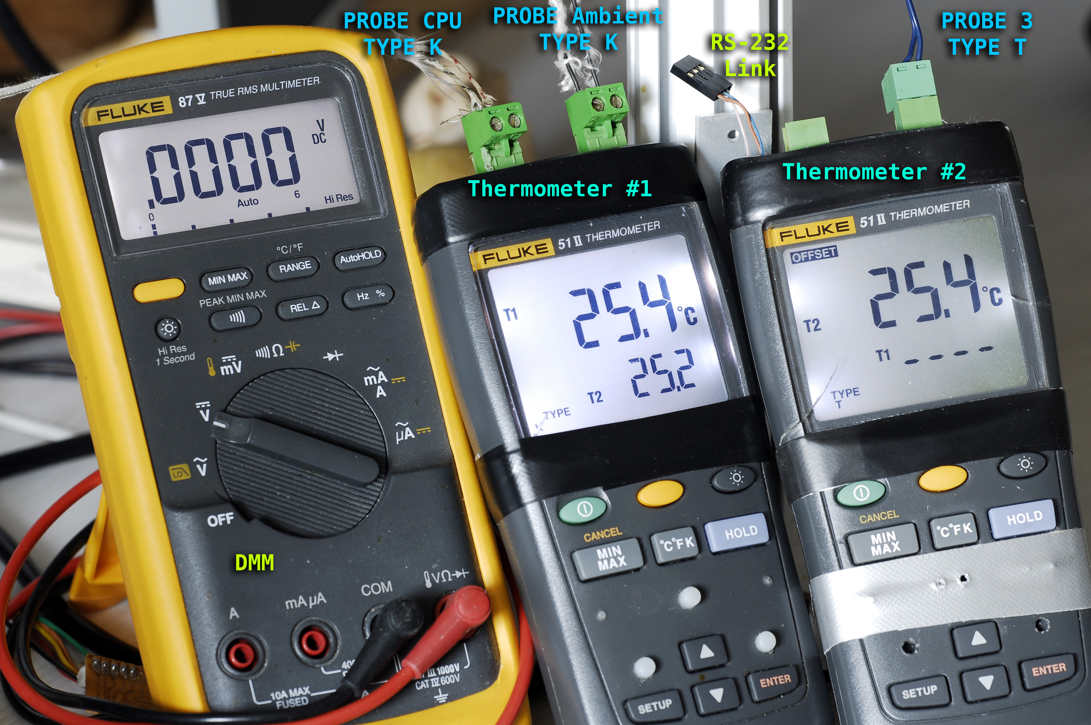
Fluke 87V True RMS DMM
Two Fluke 50 II series thermometer
So Fluke DMM will serve me as checking unit, to see what is happening with system, to make some measurements and adjust settings if needed, and as a reference meter, because it have industrial-grade accuracy (0.05% for VDC, 0.2% for resistance).
Fluke thermometers used for contact measurements of heatsinks and components, with help of thermocouples of Type K and Type T. I did modifications for these 51 II meters to achieve dual channel operation, better backlight and USB data logging ability. Data captured with speed 1Hz by 500 samples bursts, and then processed using Fluke Forms 3.5 Software. Accuracy of thermometers is 0.2% + 0.3C.
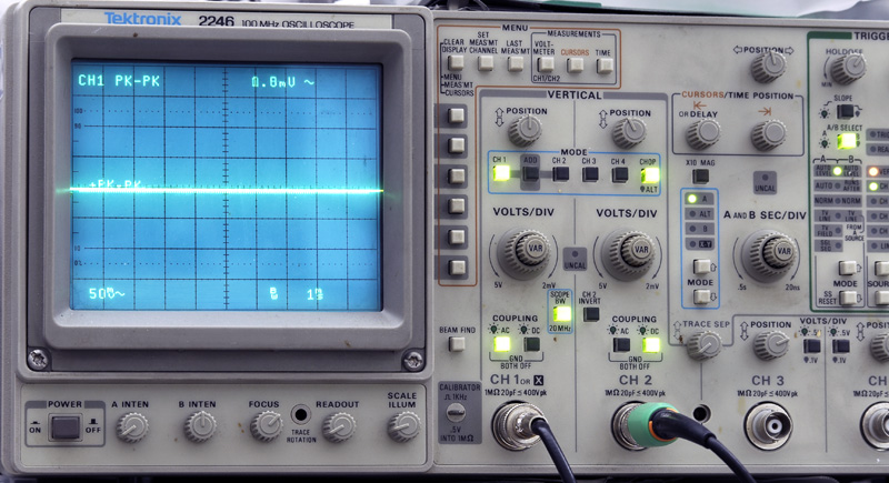
Tektronix 2246-1Y 100MHz 4-ch scope, precise analogue device, without sampling artifacts and approximation found in low-cost digital scopes. Oscilloscope was used for waveform capture, and noise measurements for further analyze. I will do peak-peak noise, level and timing signals measurements. This is 2+2 channel 100MHz analogue model. I use compensated 150MHz probe with internal 1:10 division and custom compensated probe for motherboards.
Logic analyzer using high-speed ALTERA Stratix FPGA - for PWM waveform observation and measurements. Logic analyzer will be used for digital measurements and digital bus capture, if needed. It's implemented via ALTERA SignalTap parametric module configured in ALTERA Stratix EP1S25 FPGA, able to analyze inputs with up to 300MHz. Logic analyzer uses Agilent 01650-61608 16-channel pod.
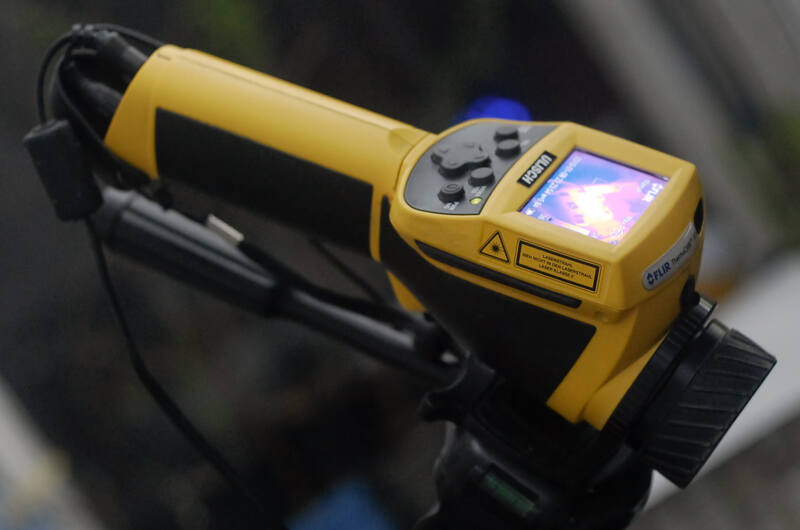
FLIR Thermacam B2 thermal imager
Nice tool to visualize thermal effects and hot sources.
FLIR thermal imager provides help thermal analysis of DC-DC circuits in Tier 3 testing.
Host PC with DAQ (National Instruments LabVIEW VI's)
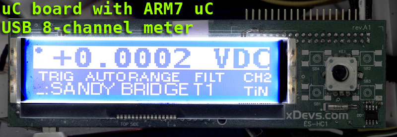
Own-made xDevs.com Neutrino ES for DC power measurements
Host PC running NI LabVIEW collect data from my custom devices used during tests, process results and show measurements as comfortable and flexible GUI. This relates to DC power measurements and voltages monitoring for Sandy bridge platform.
My 8-channel digital logging meter was also used for adjusts.
Boards overview
Before we continue with tortures and benchmarks, let’s take small tour to motherboards features and details.
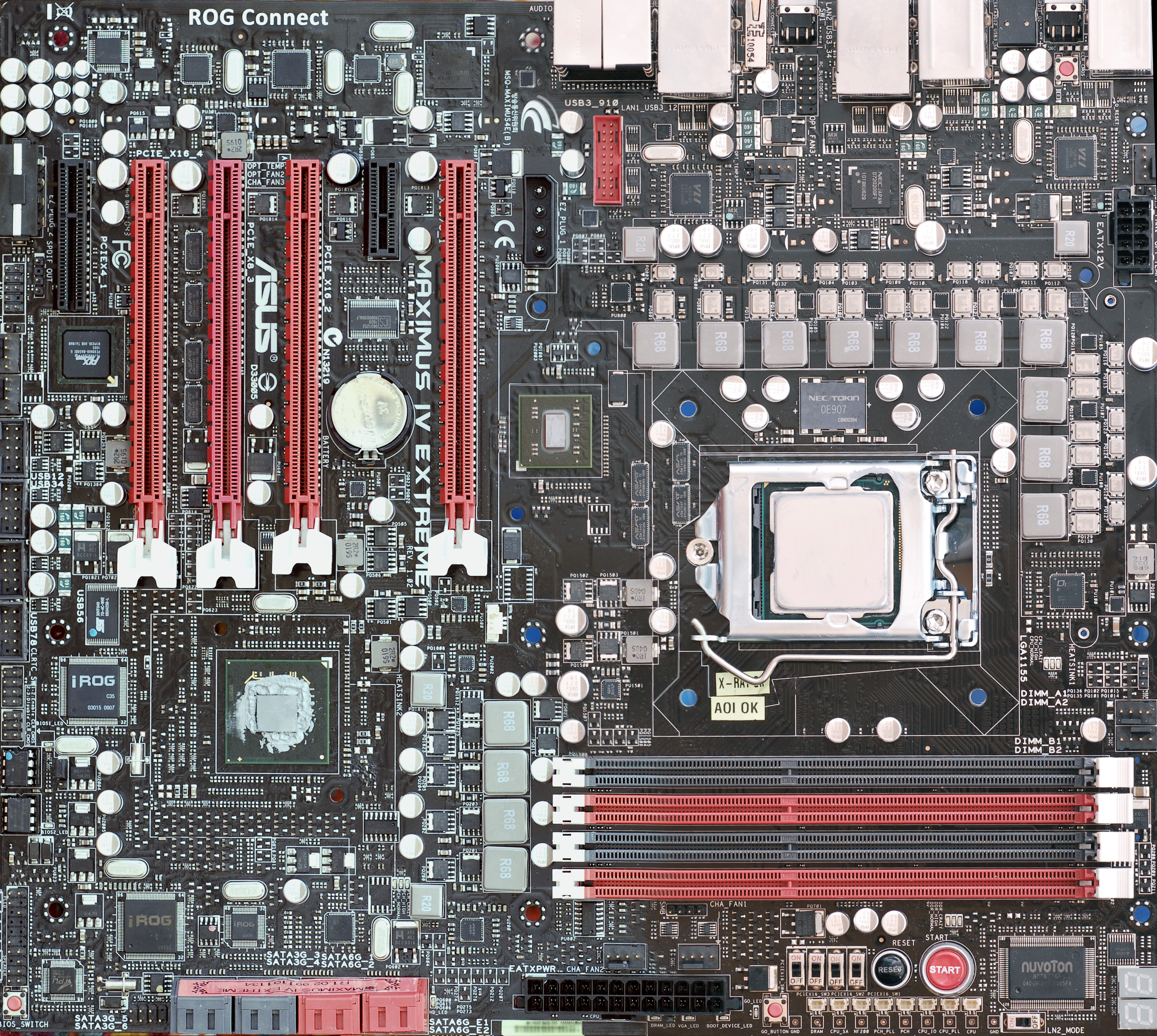
ASUS Maximus IV Extreme
Color scheme is similar to other ROG series motherboards, consists of dark gray and red colors. All expansion slots for cards are PCI-Express,
four with x16 physical size (three of them have x16 routed lanes, and one x8), one x1 and last one is x4 with open side, allowing bigger cards
to be installed. NF200 is connected to second and fourth slot. Slot latches are robust big dual-side type, which are not always comfortable to use
with tight multi-GPU setups.
Board have lots of headers for fans, two near 24-pin ATX power input, two near DIMMs, two more near PLX bridge, and two above CPU power circuitry.
Total amount is eight fan connectors, so overclockers will enjoy that. All of them are 4-pin type.
Board dimension is 305 x 269, what is called Extended ATX, so better do double check if it fit specific
enclosure. I will run everything caseless, so zero issues here.
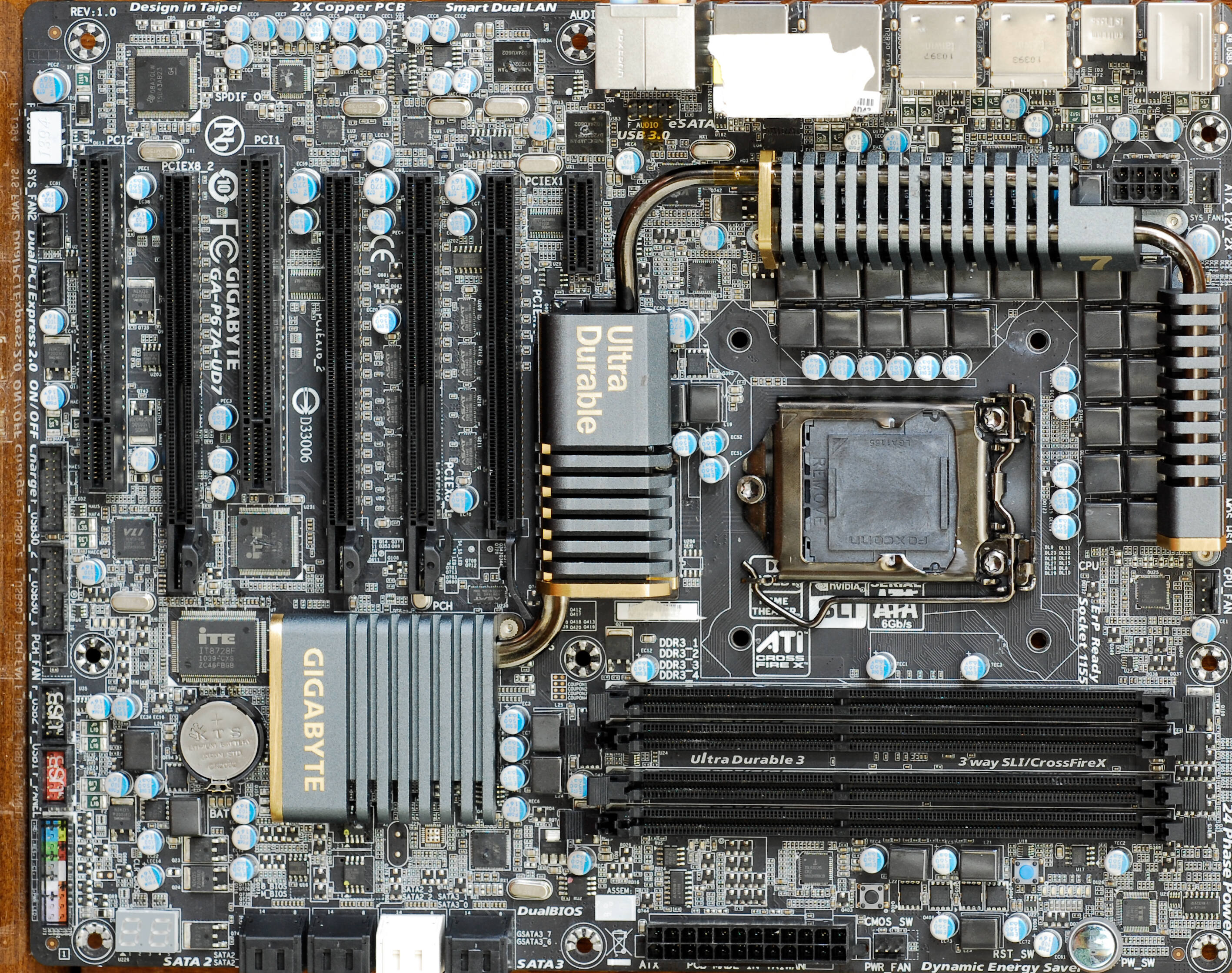
Gigabyte P67A-UD7
Gigabyte board is standard ATX, 305 x 244, so it can fit most cases easy.
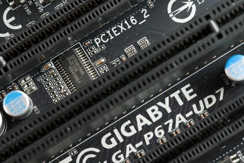
Unlike Maximus, P67A-UD7 have four physically full-size PCI-Express slots, one x1 slot, and pair of legacy PCI maintained by ITE hub.
There 6 fan connectors onboard, two of them 4-pin type, rest are legacy 3 pin.
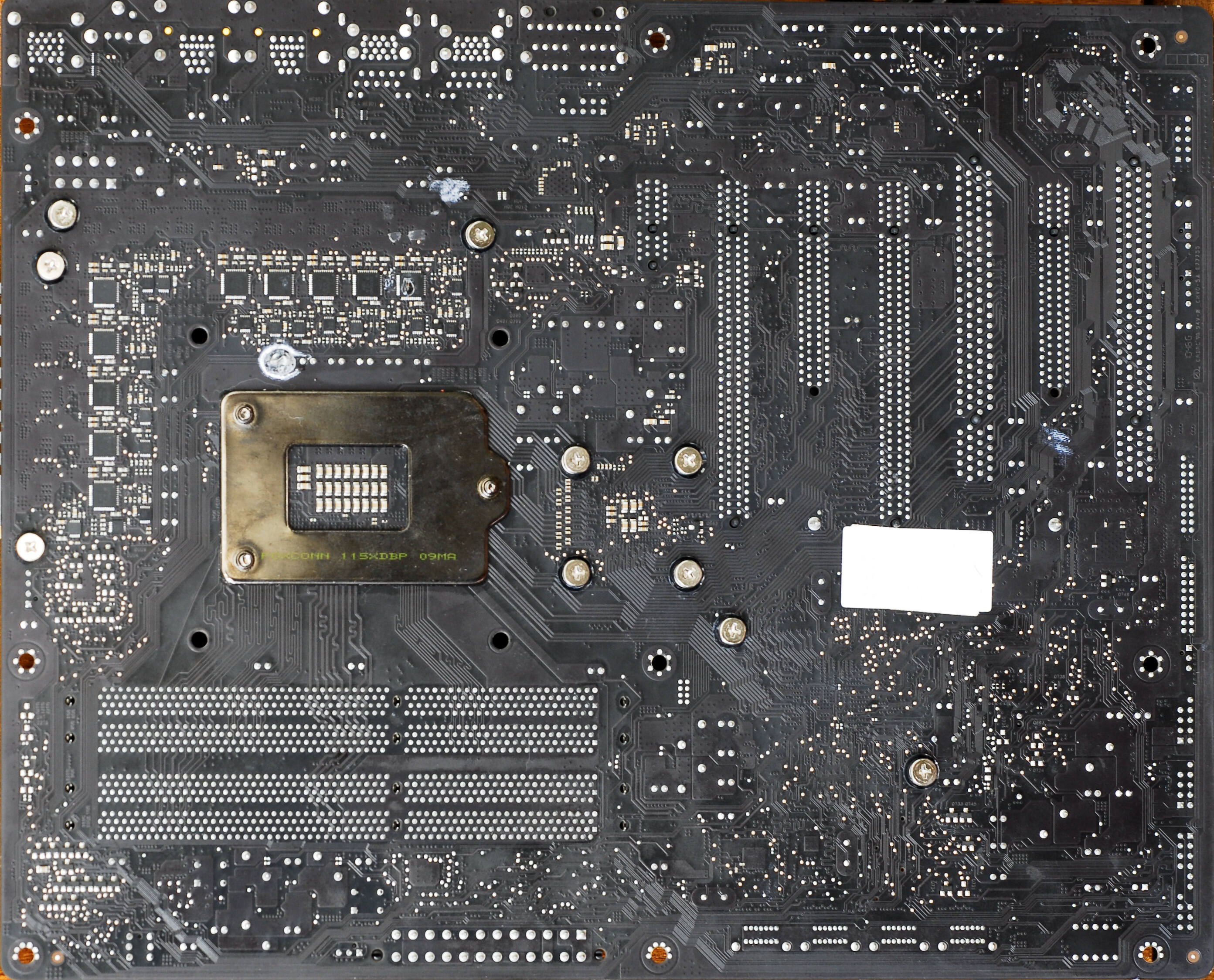
Both boards are based on Intel P67 Express chipset, with four DDR3 slots, just like most P67 boards. Both are using 8-layered PCB.
Both have debug POST 80h indicator, total eight SATA ports, some including SATA3 support, Power/reset buttons and few LEDs for monitoring.
Expansion connectors
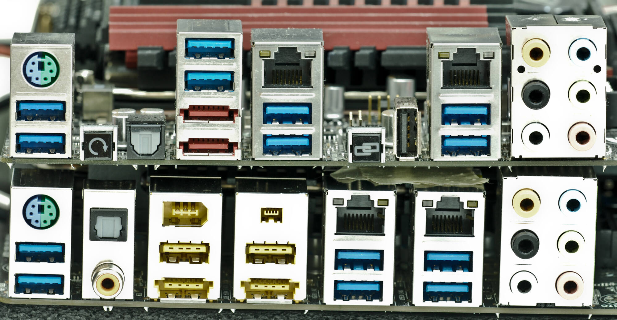
Rear I/O looks full of connectors, with nice bluish SuperSpeed USB 3.0 ports, dual GbE ports, sound, FireWire and SATA connectivity. ASUS board is on top part of image, Gigabyte - bottom. There are also CMOS clear button and remote overclocking button with featured port (vertical standing USB port). If remote OC not needed - USB port may be used just as normal one.
Circuitry analysis
Power convertors
Both boards use variety of different power DC-DC convertors. I will introduce them one by one.
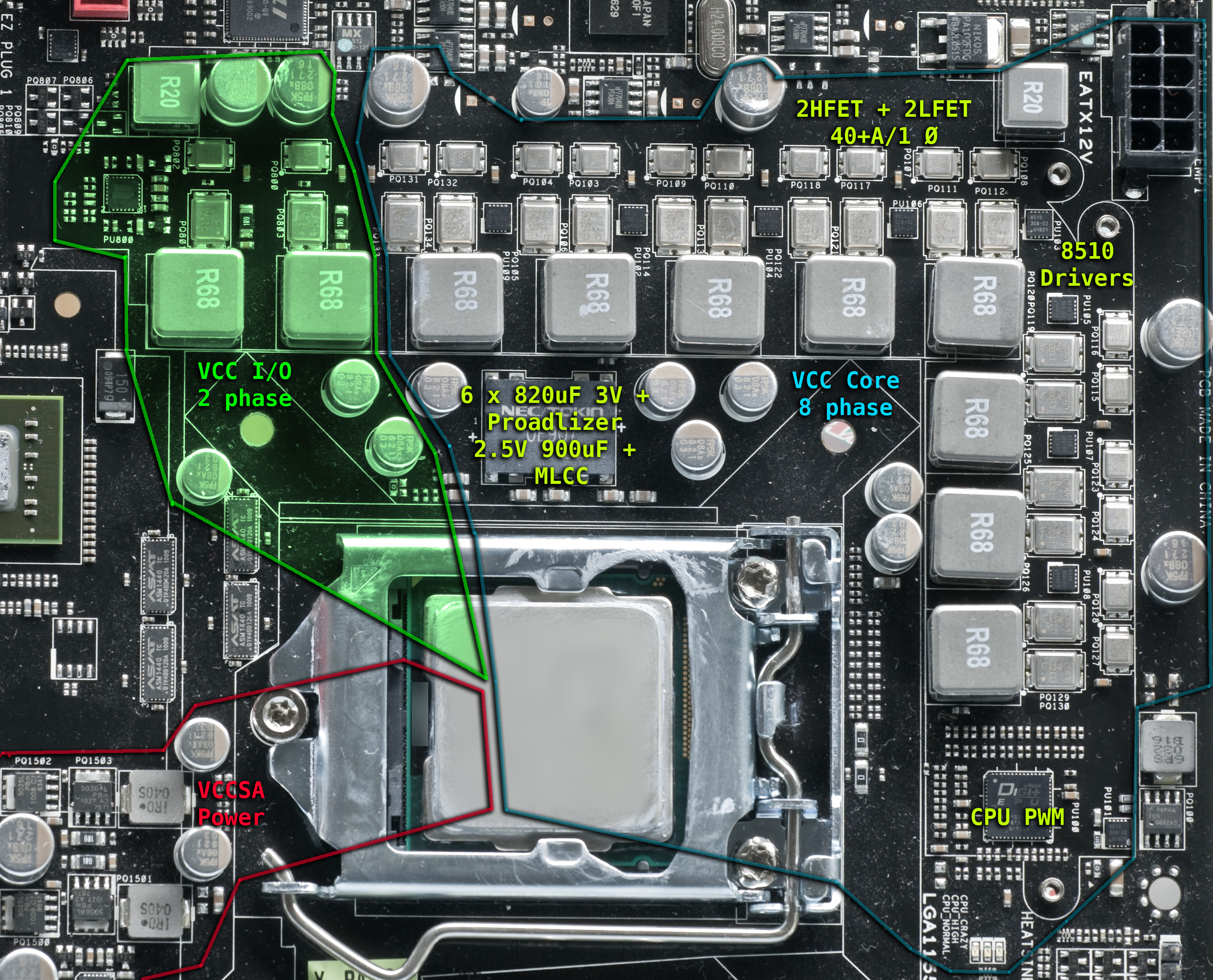
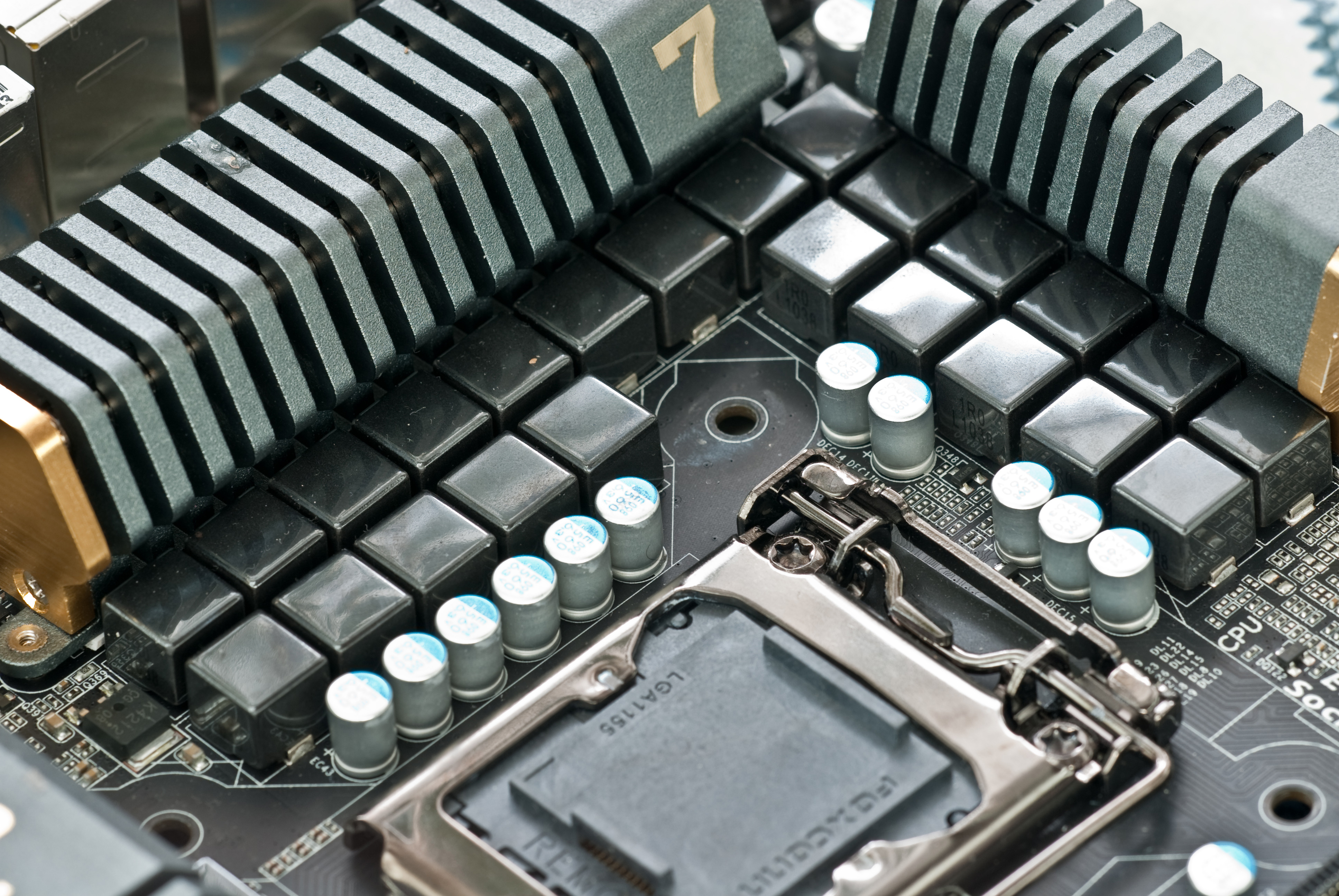
CPU VCC power - this is main CPU power circuitry which provide juice for CPU cores together with integrated GPU.
ASUS Maximus IV Extreme board
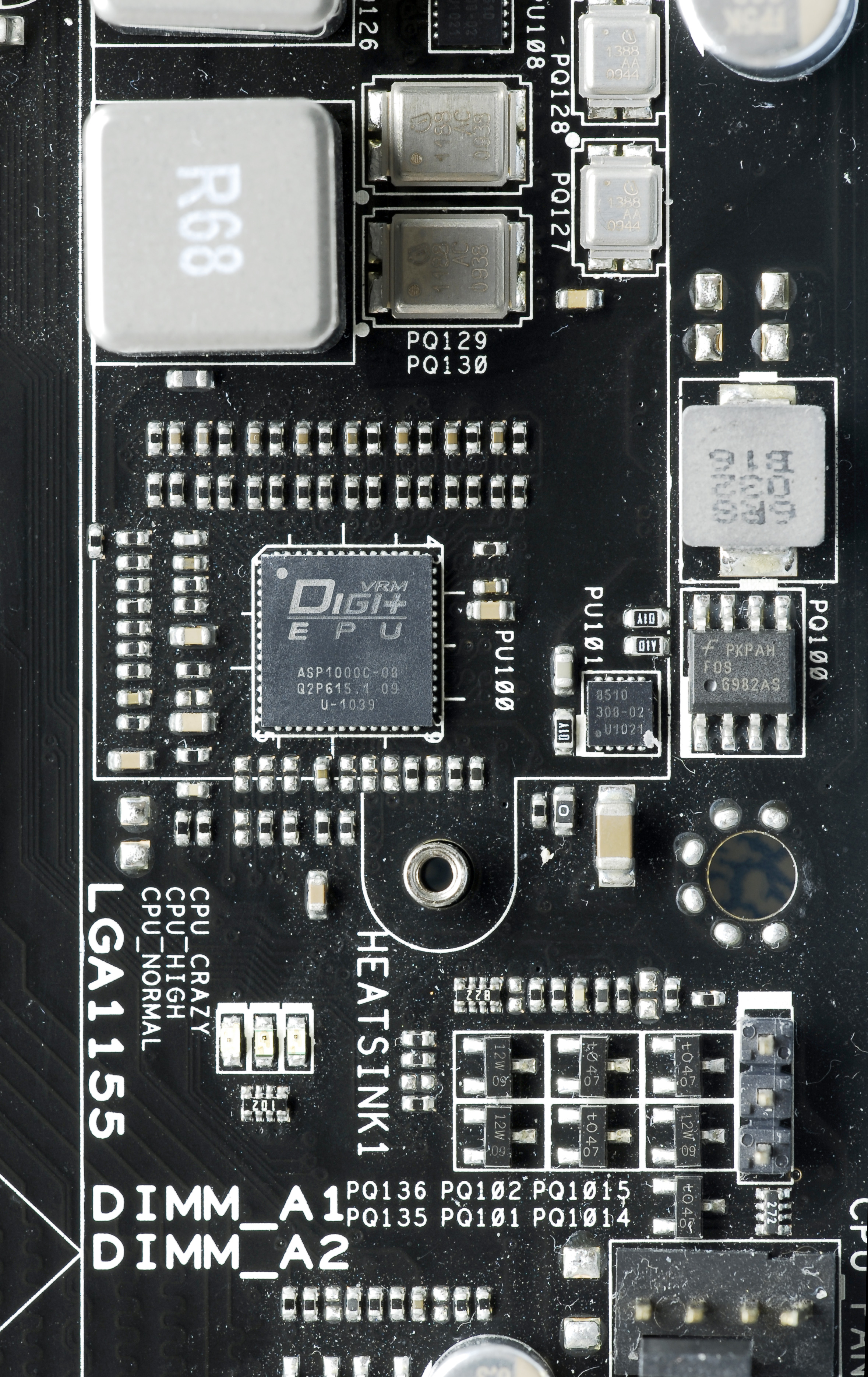
Based on proprietary "ASUS Extreme Engine Digi+" chipset.
Actually it uses CHIL drivers (CHL8510) for phase control, so looks like it's CHIL PWM solution adapted for ASUS use. Convertor is built using high-frequency 8-phase design with synchronous buck topology with extensive voltage and current control. This advanced VRM is able to run at high switching frequency near 1MHz.
Each phase consists of four (one pair for high-side, second pair for low-side) Infineon mosfets in advanced metal CanPAK packages. These transistors have very low resistance in active state, thus reducing parasitic power loss and enhancing efficiency. Also metal package allows much better thermal dissipation, lowering operation temperature. There is good public illustration compared to SO-8 MOSFETs. More efficiency and better cooling mean that more power can be transferred to load without critical overheating, which is essential in case of overclocking. Such components are already seen on high-end motherboards and videocards, like Rampage III Extreme, custom-designed Fermi videocards.
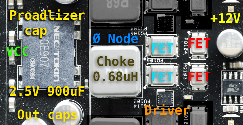
Output inductors used seems like metal alloy Trio LM-68B, 0.68uH with rated current 28A per each and 1.38 mOhm DCR.
Each phase is controlled by dedicated driver in small lid-less package nearby. Drivers converting PWM signal from main power controller to driving signals for discrete MOSFETs. Using driver chips allows engineers to simplify design of high-current switching power supply by reducing length of driving signals, and adding more sophisticated control and protection circuitry to overall system. Back side of VRM covered by aluminum heatsink plate, just for better thermal.
Power from input +12V rail decoupled in four low-esr input capacitors, 270uF 16V each. Output power plane for CPU Vcore have total bulk capacitance about 5820 uF, consisting from 6 low-esr aluminum can capacitors (820uF 3V each) and one NEC/TOKIN Proadlizer PF/A cap with 900uF 2.5V rating. These polymer capacitors help to reduce fast transient spikes and have very low ESR, about 1.5 mOhm by spec.
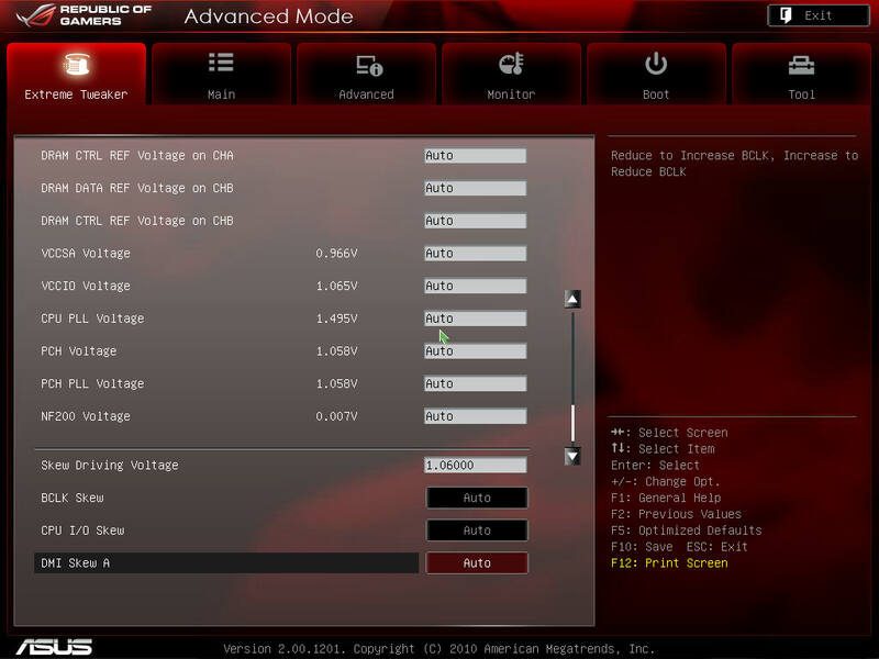
This voltage adjustable from BIOS, in range 0.800 to 2.155V, with 5mV step.
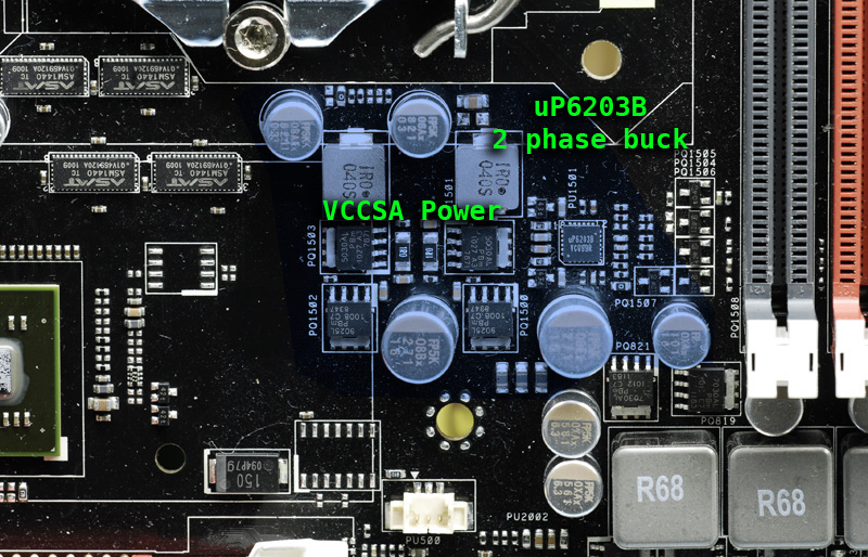
CPU VCCSA power
System agent is a part of Sandy Bridge CPU which controls communications, in a way like legacy northbridge did. SA is not as power hungry device as CPU cores so it take power from simple synchronous buck DC-DC based on uP6203B and pair of phases. Each phase feature NXP PH5030AL NFET and PH9025L for high side. Both FETs able to push more than 60A.
Input capacitor - 2 x 270uF 16V, output - two 820uF 3V caps. Each phase use small 1uH inductors for energy storage.
This voltage adjustable from BIOS, in range 0.800 to 1.7V, with 6.25mV step.
CPU VCCPLL power
Phase-Locked Loop autotunes adjustable frequency source to have stable and precise clock output. It is used widely in digital systems to multiply/divide clocks, filtering and clock recovery. Its power should be as clean as possible to have highest stability achievable. PLL's don't need lots of energy so on ASUS Maximus IV Extreme it's powered by small DC-DC.
This voltage adjustable from BIOS, in range 1.200 to 2.2V, with 6.25mV step.
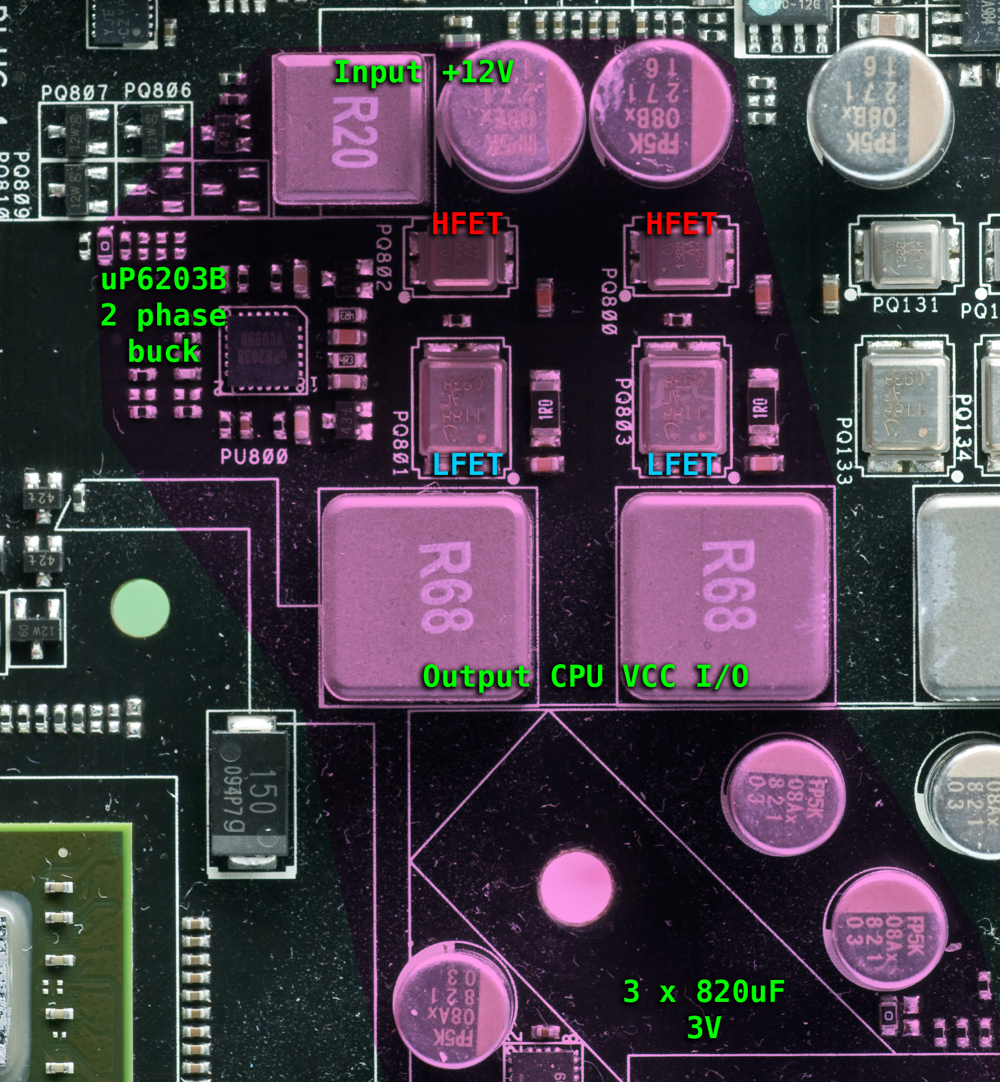
CPU VCCIO power
CPU internals like cores or GPU use low voltage for operation, but output signals usually driven at 1.5-1.8 or more volts, like DDR3 memory chips or PCI-Express signaling. So I/O voltage is taken externally and used as base level for external interfaces. This voltage was often called VTT/QPI, VTT/DRAM etc on previous P55 and X58 chipsets. VCCIO usually affects DRAM overclocking and memory controller performance, like in older platforms before Sandy Bridge. It's fed by quite decent 2-phase synchronous buck controlled by uPI Semiconductor uP6203B. Except the DC-DC controller, both phases use same components as main Vcore VRM. Input capacitors include two 270uF LowESR 16V and output is decoupled by 3 x 820uF (2460uF total).
This voltage adjustable from BIOS, in range 0.800 to 1.7V, with 6.25mV step.
So there are quite a few main power sources for Sandy Bridge CPU's.
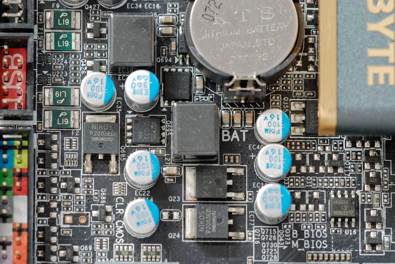
DRAM VCC power
Memory sticks take power from triple phase power supply with 0.68uH coils, powered by PH7030AL + PH7030AL NFETs. Each FET can push 50+ A current. Power supply controlled by uPI uP6207. There are four input capacitors, 560uF 6.3V each, and eight 560uF 6.3v for VDIMM plane. Total decoupling capacitance for memory is near 4500uF, making DIMM voltage solid and steady.
This voltage adjustable from BIOS, in range 1.200 to 2.2V, with 6.25mV step.
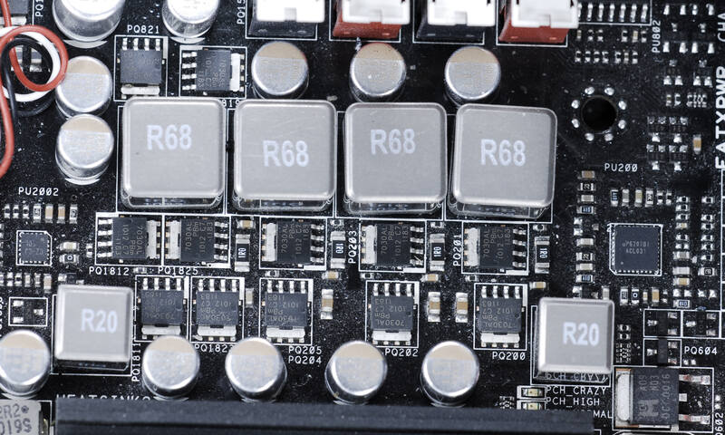
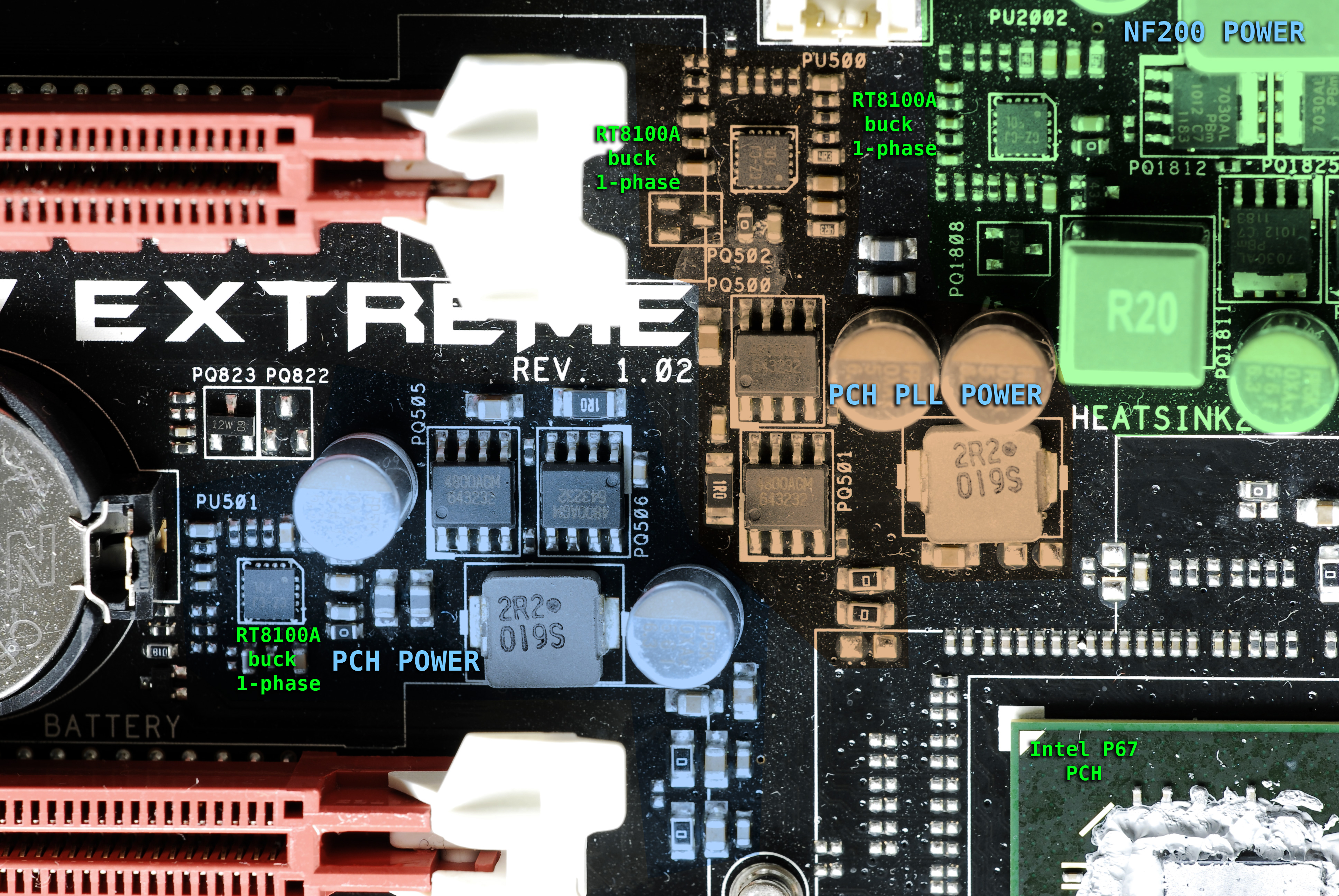
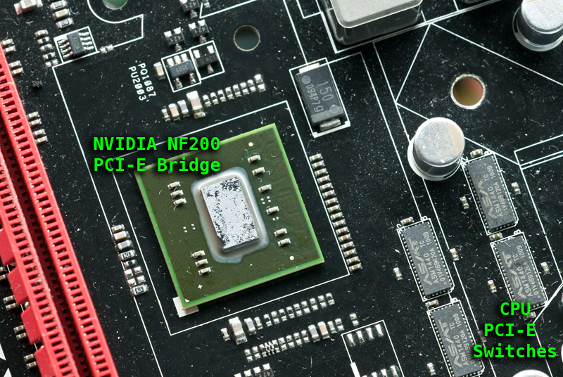
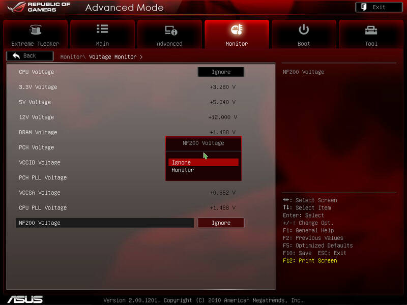
NF200 power
Use single phase maintained by Richtek RT8100A. Phase feature doubled PH7030AL pair (2 FET for high-side and 2 for low-side) and 0.68uH inductor similar to those used in VDIMM, VIO and Vcore convertors.
Nice feature present on ASUS Maximus IV Extreme - power disabled by hardware for NF200, so it will not produce any heat air when not used. Until you put PCI-E card into second or fourth PCI-Express slot - it's totally disabled.
This voltage adjustable from BIOS, in range 1.1925 to 1.5105V, with 13.25mV step. Standard voltage level for NF200 is 1.2 V.
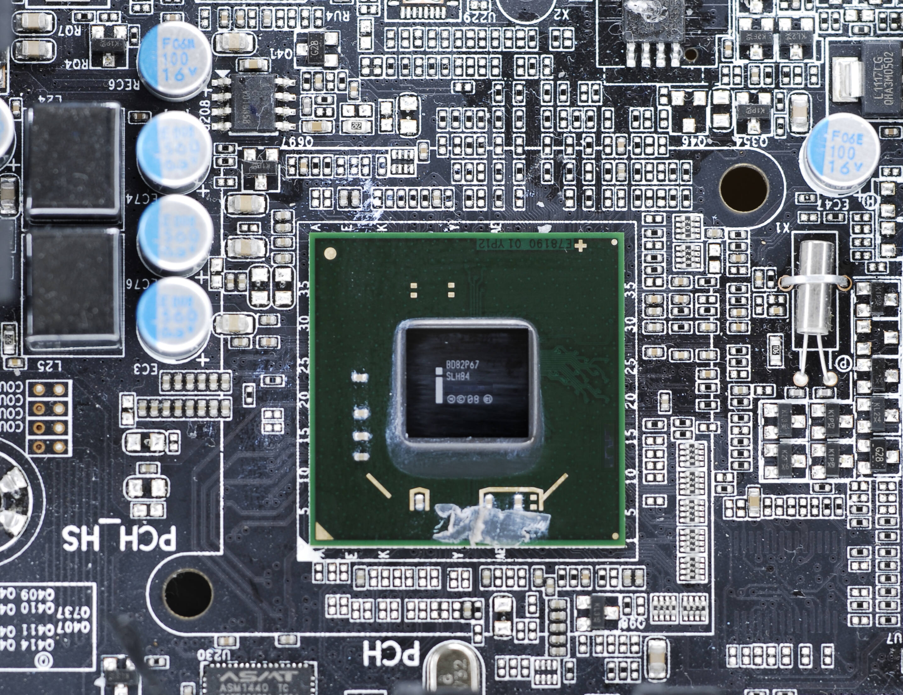
PCH power and PCH PLL
Similar to CPU PLL, but used for clock conversion in PCH.
Use two RT8100A-based single-phase convertors, with pair of 4800AGM N-channel FETs in SO8 package. No need for insane power here.
Inductors used in both convertors are 2.2uH.
PCH and PCH PLL voltages adjustable from BIOS, in range 0.80825 to 1.70925V, with 13.25mV step.
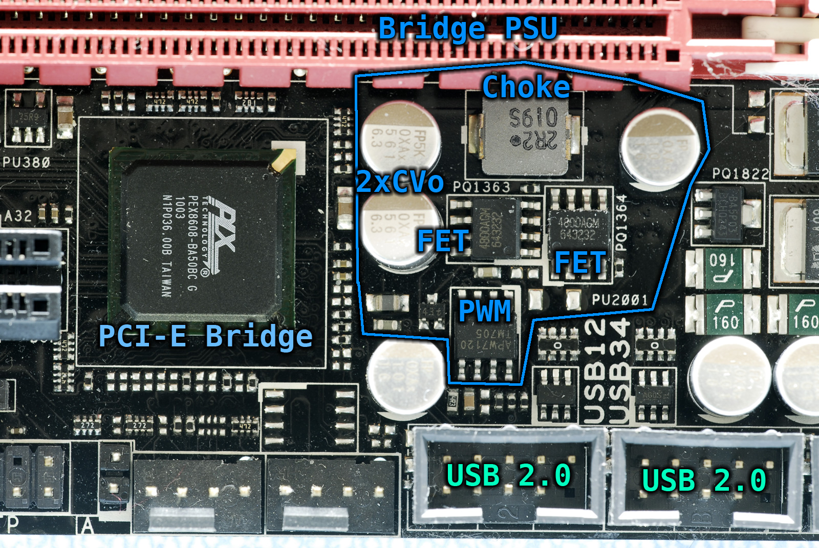
PLX Bridge PEX8608 uses APM7120 controller for its power. In rest it's same as PCH power power solution. There is pair of 560uF bulk caps for decoupling near by. It's voltage not adjustable from BIOS.
Extra onboard controllers, like integrated sound-card, Super I/O chip, Ethernet chips, SAS/SATA, USB controllers usually need small amount of power, so they fed by simple linear low-drop regulators (LDO's) similar to LM1117. Output voltages usually vary from 1.2 to 3.3V.
Add-on ports and controllers
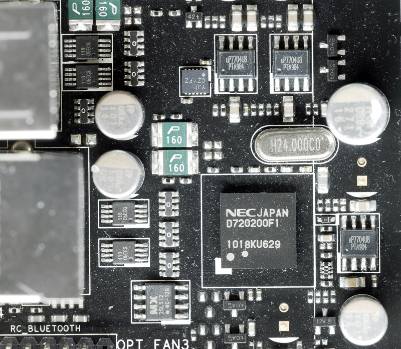
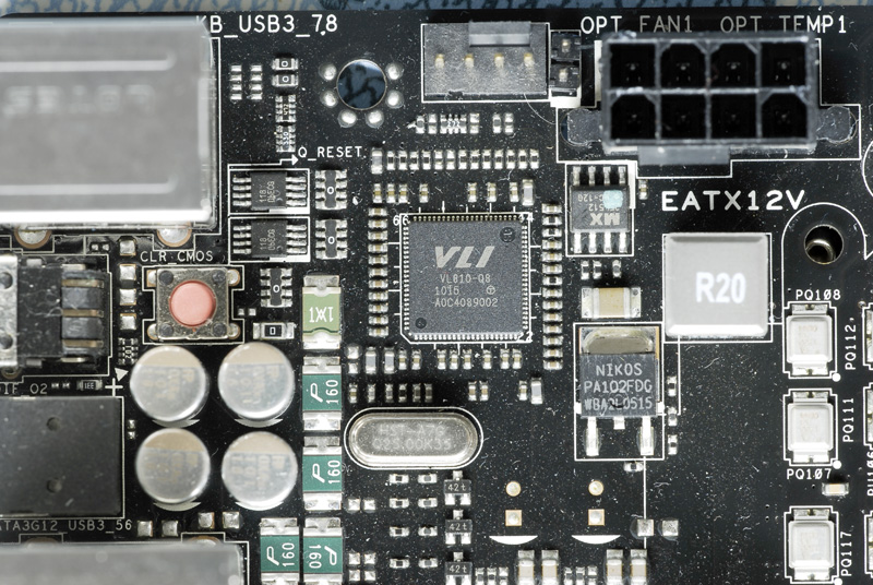
Both boards have USB 3.0 NEC hub, well known already by P55/X58 boards with SuperSpeed ports.
ASUS also choose to use quad-port VIA VL810 hub switch made with 80nm node tech process.
Let's switch to Gigabyte high-end motherboard for Core i7 2000 series CPU.
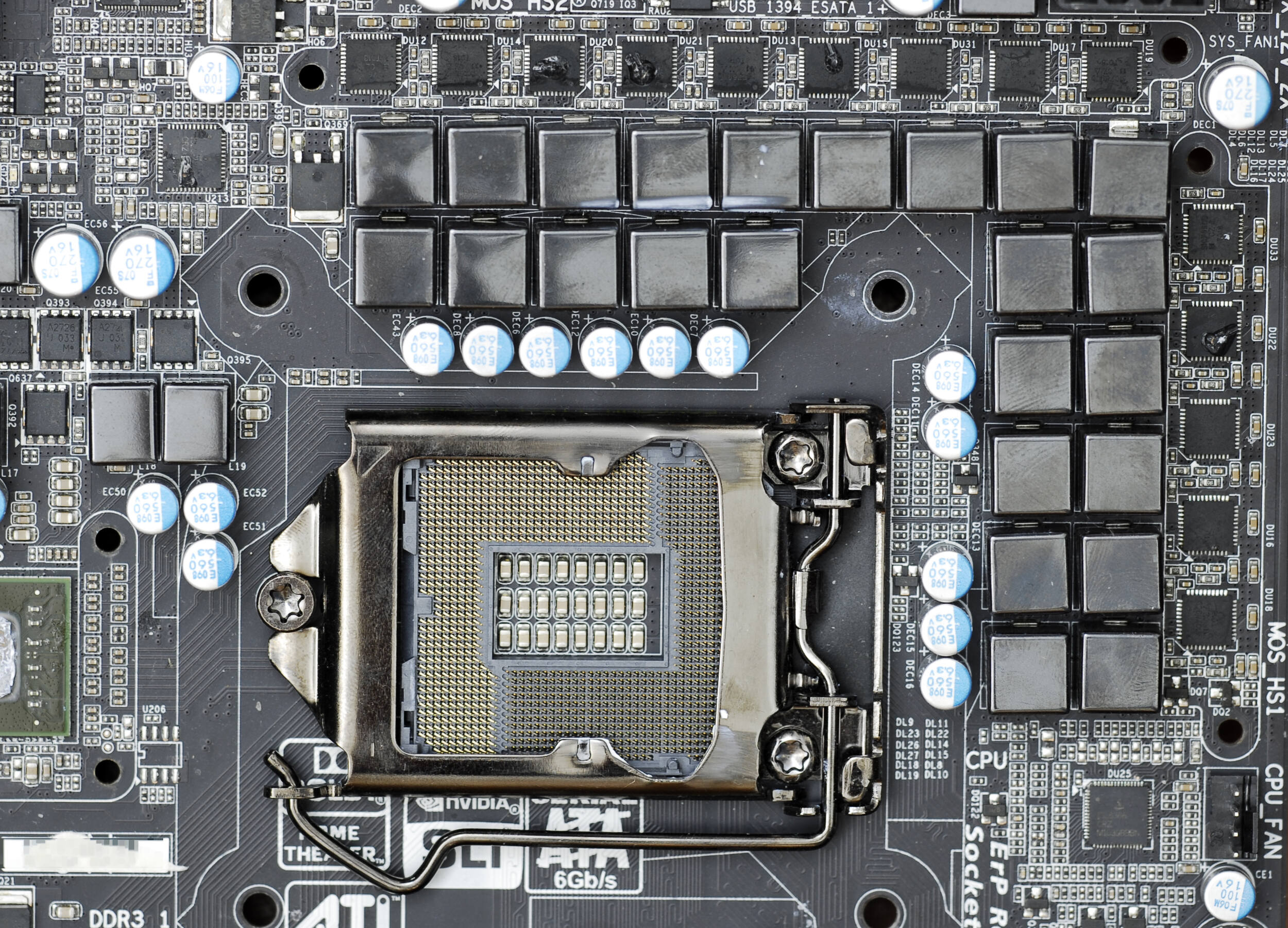
Vcore
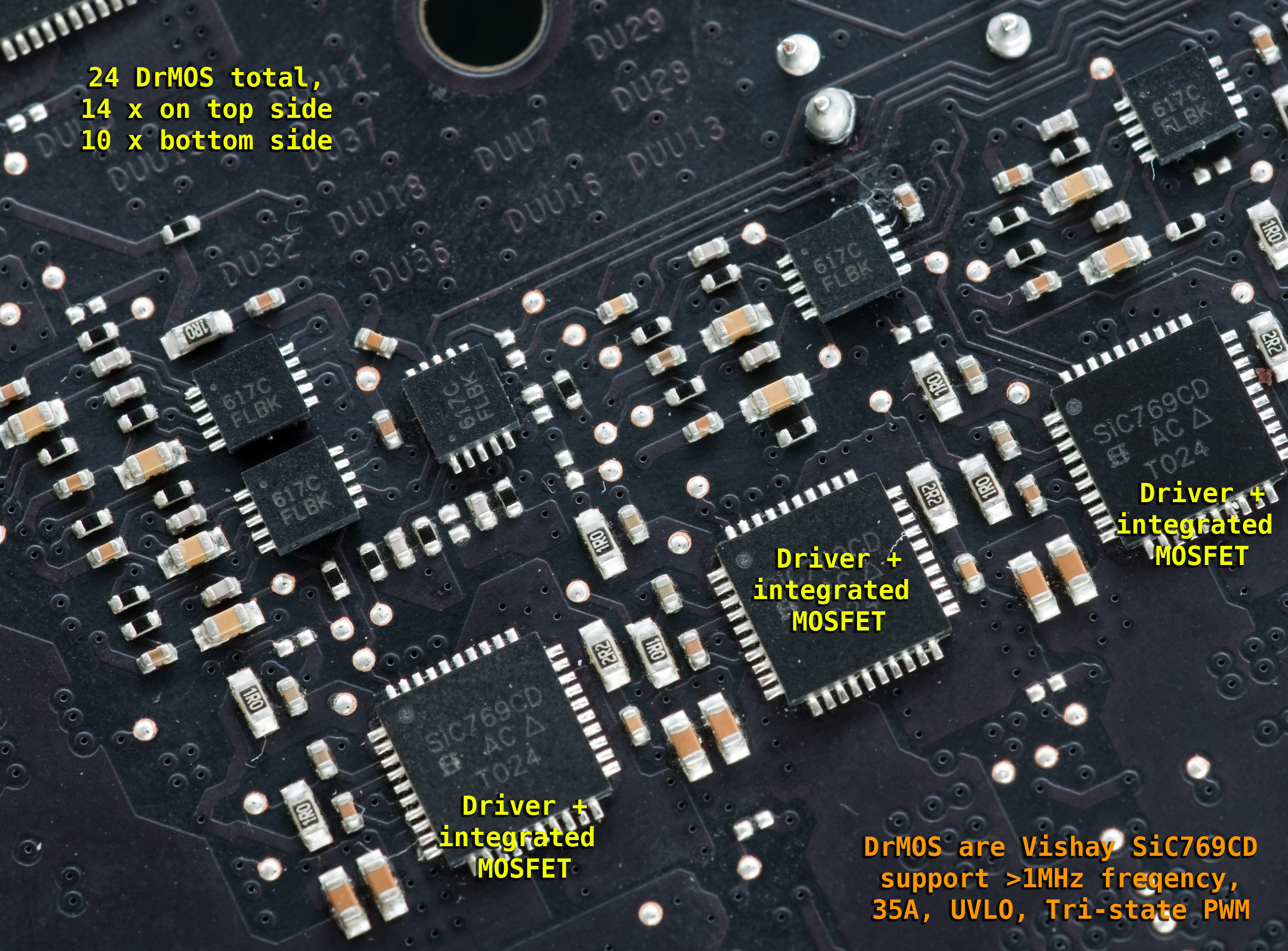
Main VRM covered under nice-looking heatsink with "7" labeling. UD5 have blue decoration and "5"
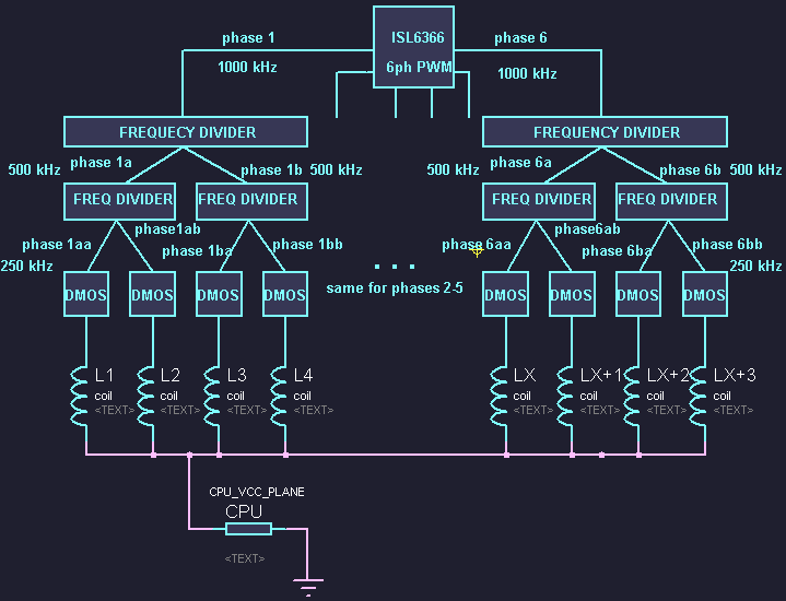
Lots of inductor coils. Lots. 24 of them. Looks great, but none of consumer PWM power controller support 24 phase operation directly. Most advanced devices, like Volterra 1185MF able to control 10 phases. So we have here phase split, when one PWM channel used to control more than one physical buck circuitry. By simple calculation we get here 6-channel PWM topology.
6 real phases * 2 (double) * 2 more = needed "24" phase. But if you add something at one side, it's always a sacrifice in something other. Let me show schematic view, where topology will look like this:
There is no technical need to make such complex system. Having more phases does not mean that CPU will get more power. Multi-phase systems made because it's simpler to spread big high-current load to separate nodes, so each node converts only part of whole power needed. But having too much nodes may lead to excessive noise and voltage deviation, because it's more difficult to control many nodes with high-speed PWM channels. As in general it's better to have some golden middle solution.
So Vcore for CPU is controlled by Intersil ISL6366 chip. PWM signals go to frequency divider (small chips with 5 pins each side, labeled 617C FLBK). Frequency divider takes input signal, in our case 1000kHz from ISL6366 PWM channel and make two output signals with half frequency (inverted+normal). Then these two outputs are divided again by two more frequency dividers, whose outputs are finally drive DMOS chips at 1/4th frequency of original input PWM signal, 250kHz in out case. Each DMOS chip is a hybrid IC with two MOSFETs and their driver. So each PWM channel from ISL6366 flow thru three dividers to reach MOSFET gates. Frequency is always 1/4 of PWM phase. So with such unit it's impossible to archieve fast rate 1MHz, as on "true" multi-phase PWM topology. DMOSes used are Vishay SiC769CD, each rated to 35A.
So looks like customer pays his dollars for lots of inductors, power chips, passives just to have nice looking thing, but not for actual performance. We will check if this statement true or false during practical test.
Quite crazy to make such a complex topology, if you ask me
Voltage adjustable from BIOS, in range 0.750 to 1.700V, with 5mV step. 1.7V may be too low for real extreme guys.
CPU PLL power
CPU PLL voltage is adjustable in range 1.52 to 2.52V, with 20mV step.
System agent power
SA Voltage is adjustable, in range 0.655 to 1.305V, with 10mV step.
DRAM power
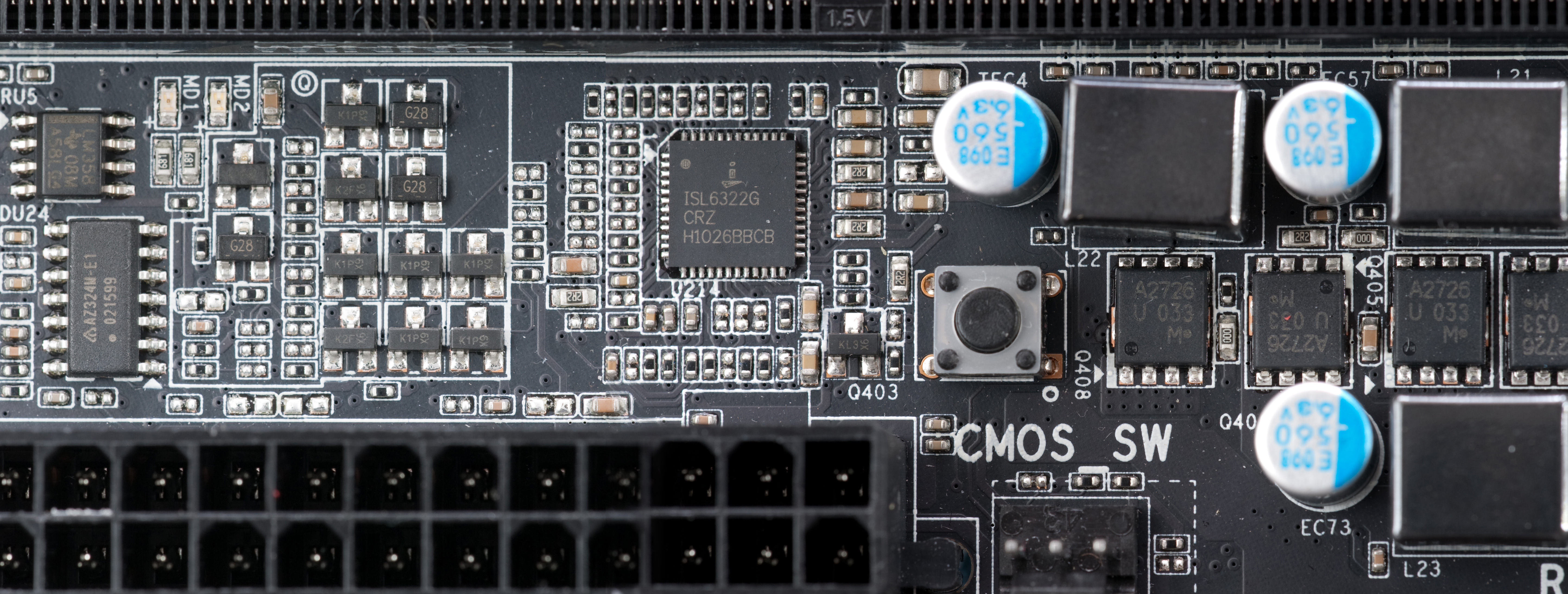
ISL6322G does work for powering memory sticks. It have dual phases to convert power, each with Renesas µPA2726UT1A FETs. Nothing interesting else to say about, this PWM chip is already known by other Gigabyte boards and high-end videocards.
This voltage is adjustable under name DRAM Voltage, in range 0.9 to 2.6V, with 20mV step.
For VIO power UD7 uses similar ISL6322 paired with two phases. Mosfets in each phase are Renesas µPA2726UT1A. Each FET can push 20A.
Input capacitance is 2 x 270uF 16V, output is decoupled by three 560uF, total 1680uF.
In Gigabyte's BIOS this voltage is adjustable under name QPI/Vtt Voltage, in range 0.8 to 1.7V, with 20mV step.
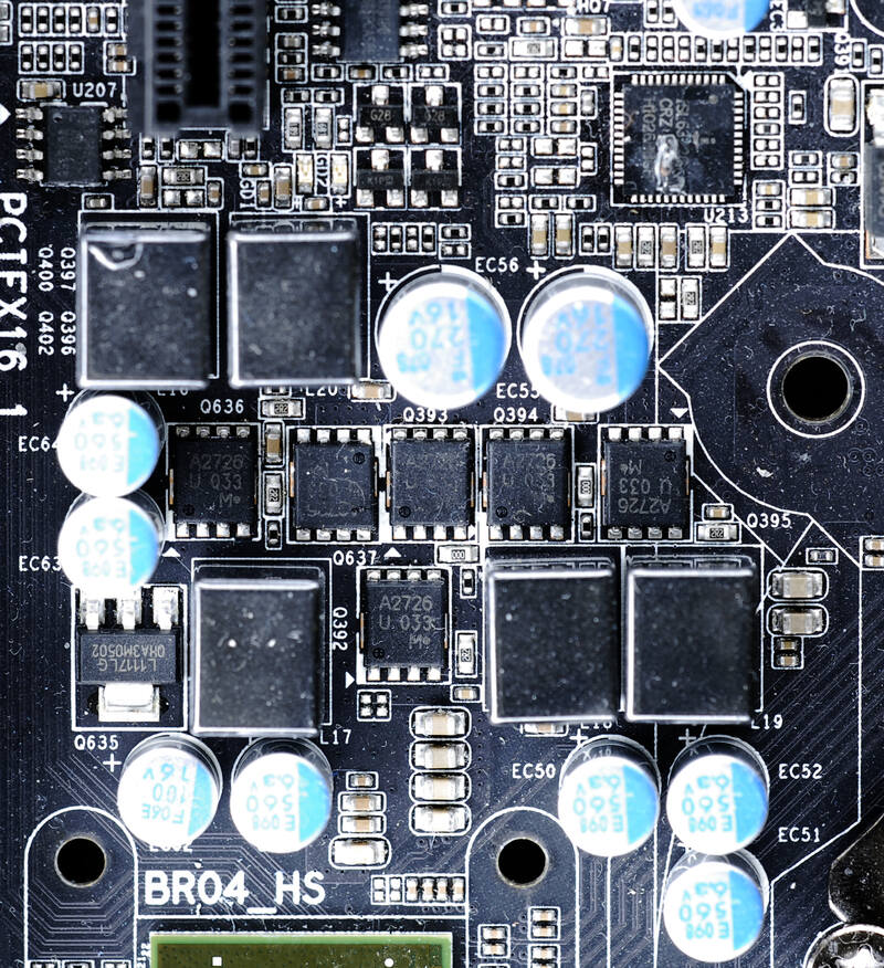
Also NF200 power placed nearby, controlled by simple 8-pin PWM Controller ISL6545 and single phase with pair of same µPA2726UT1A.
Output decoupled by three 560uF LowESR caps.
PCH power is maintained by simple PWM controller, maybe ISL6545, hidden under CMOS battery holder, with two Renesas FETs and few 560uF caps. Had no need to desolder battery holder to read PWM marking.
In BIOS this voltage is adjustable under name PCH Core Voltage, in range 0.84 to 1.94V, with 20mV step.
Features
I think most reviewers already covered widely known things about new platforms, so just stop by on most interesting things.
ASUS Maximus IV Extreme
Board have PCI-Express Gen2 differential buffer IDT 9D403DGLF to drive down-stream PCI-Express cards.
Well known NVIDIA NF200/BR04 bridge used to add two more PCI-E slots to Sandy Bridge platform.
NF200 and CPU VRM circuitry cooled by single heatsink assembly. Cooling solution is low-profile and aligned well.
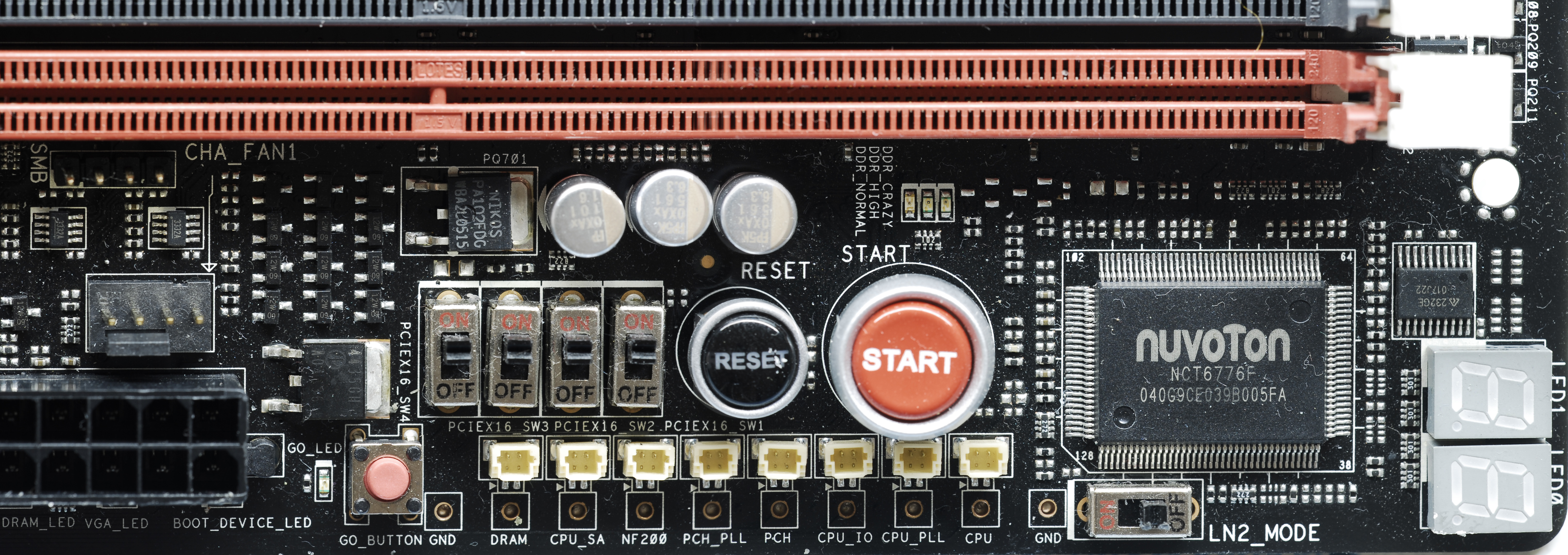
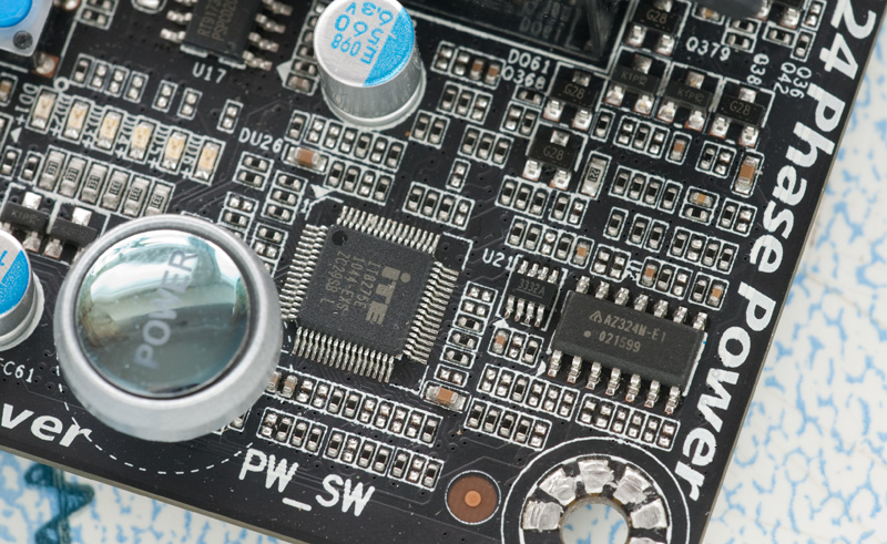
Overclockers like buttons for power and reset onboard. Also voltage check points are useful during extreme testing and for controls. Just a note here - fine-pitch connectors for monitoring cables is not a solution for most of guys, MSI ones for regular DMM probe are much better in term of usability.
LN2_Mode switch will allow easier overclocks under subzero by idea, but seems doesn't work actually on Sandy Bridge CPU's.
There also cool PCI-Express disable switches, to power down PCI-E card installed in selected slot. We saw similar idea
on Classified high-end boards. Should be nice feature for those who push hard 2-way/3-way SLI/CF rigs. GO_BUTTON loads profile from BIOS on-fly.
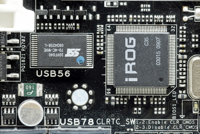
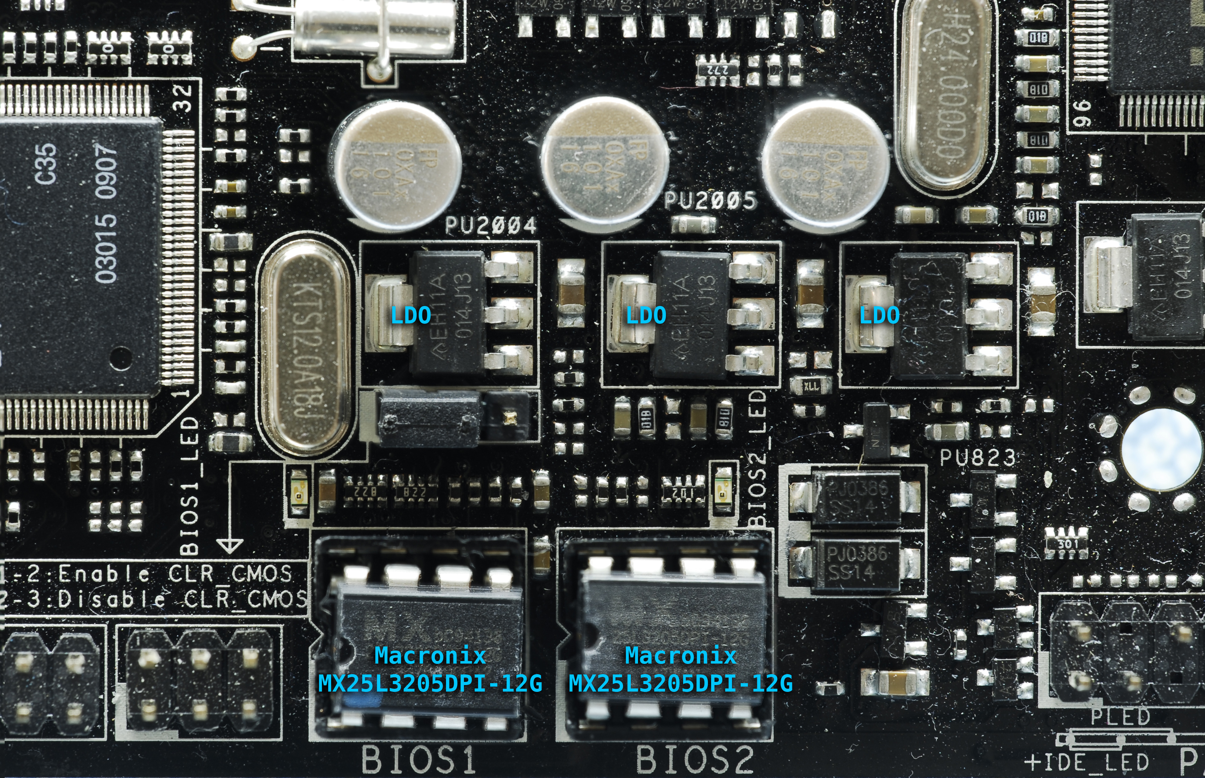
Some iROG controller which does something useful for enthusiasts. It has NOR flash chip near to store some data, maybe OC profiles etc.
Maximus equipped with two BIOS SPI Flash chips. I like also LED which show currently selected and used BIOS. Visible and usable.
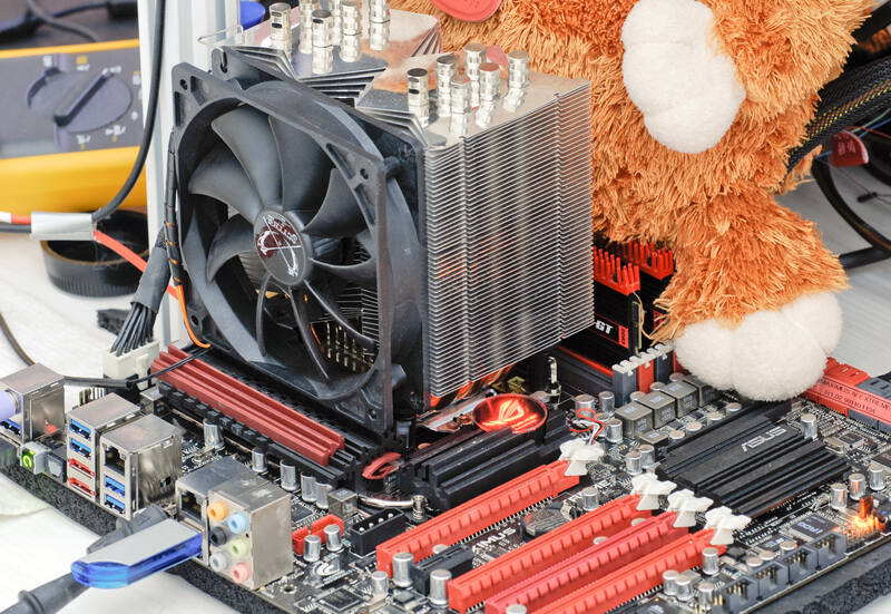
Overall platform view with cooling installed:
Gigabyte P67A-UD7
Marking with 8 layers of copper stack up.
Passive heatsink have nice look and does its job just ok.
PCH area crowded by lots of 0402 resistors, capacitors and discretes. PCH chip does not have any visible from top "bridges" or straps to solder on
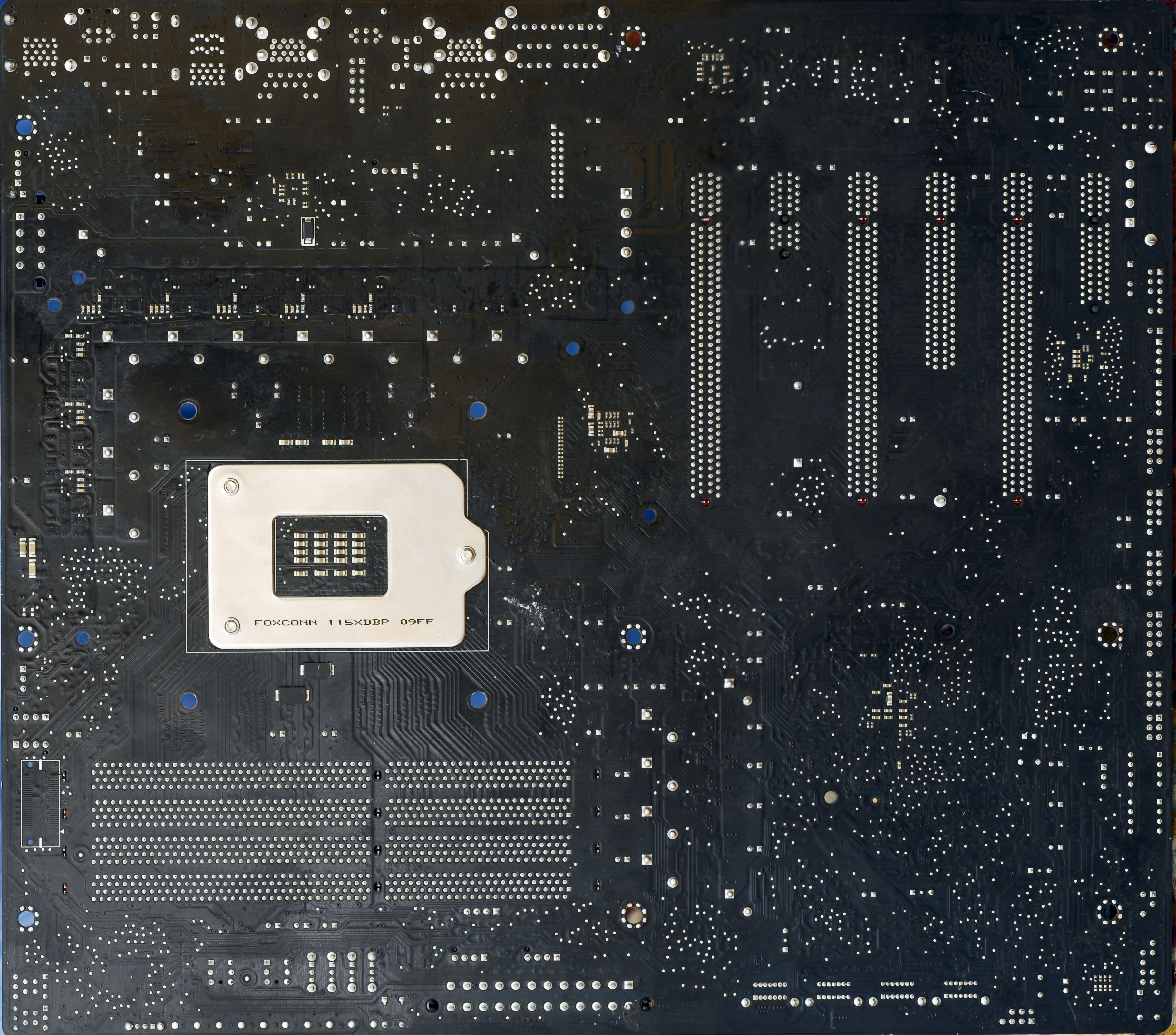
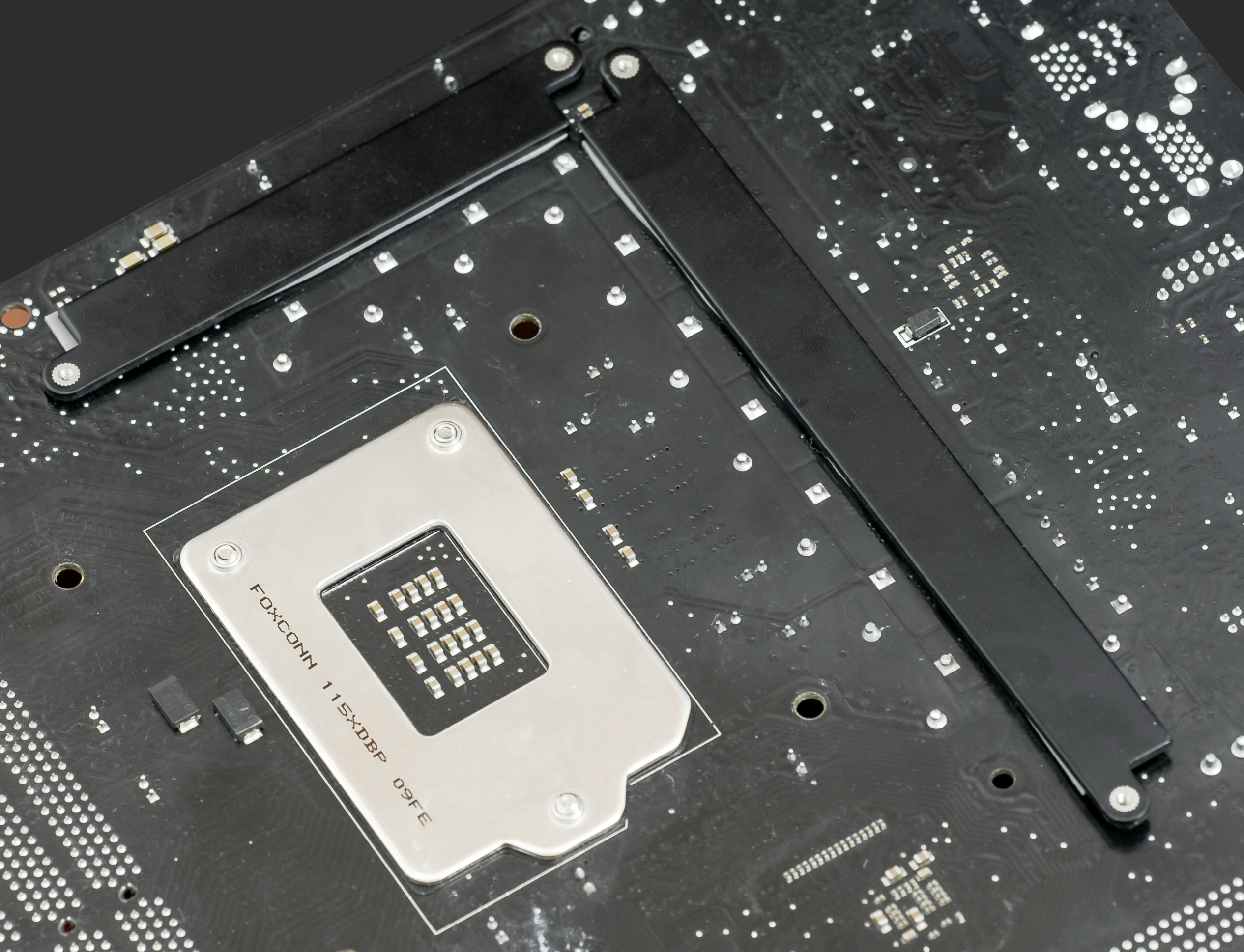
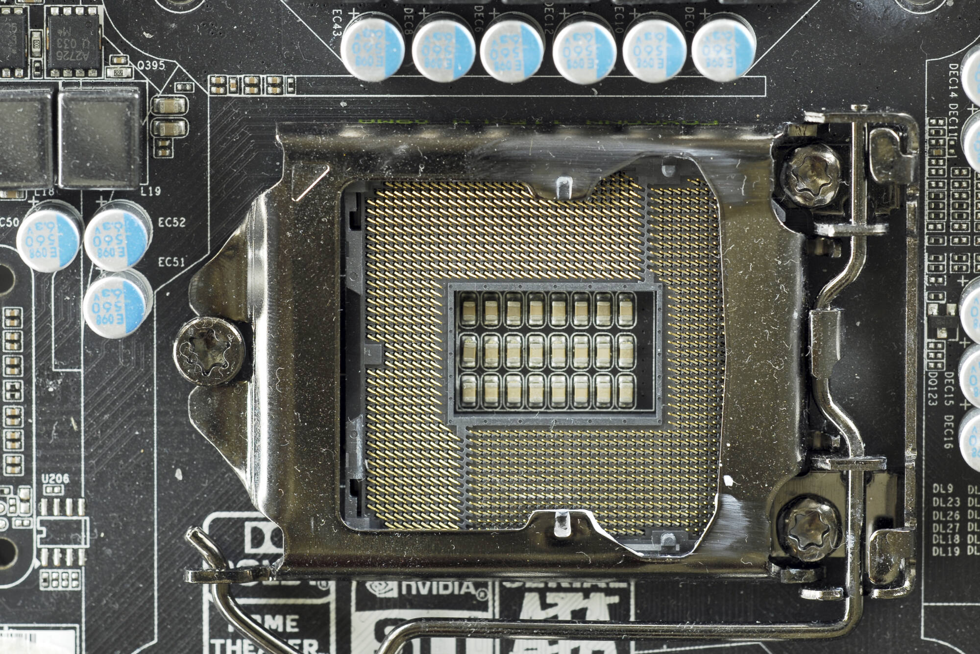
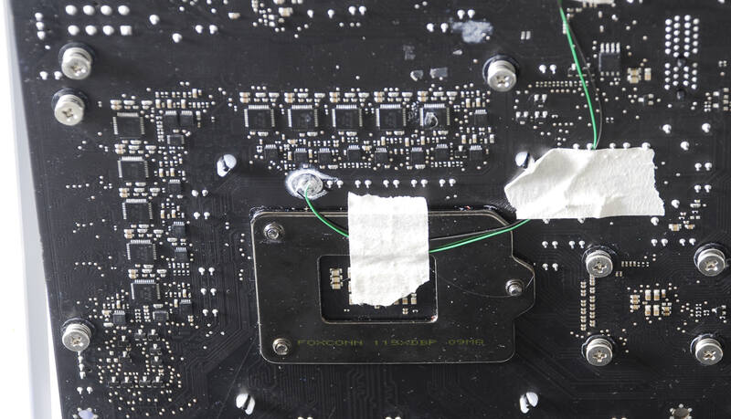
Same as ASUS board, here is used Foxconn socket. Time will show if socket burns affect 1155 platform.
UD7 have two PCI-Express Gen2 differential buffers IDT 9D403DGLF which take source clock and drive to PCI-Express down-stream devices.
PCI-Express slots use NF200 even if not connected to, so it's always heating here. Slots locks are comfortable and easy to use, much better that ASUS big ones.
Board also have power button, reset button and clear cmos button, but no hardware monitoring points.
I guess UD9 should be black-styled
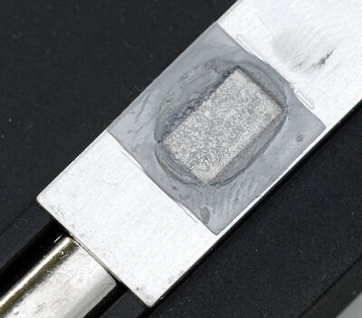
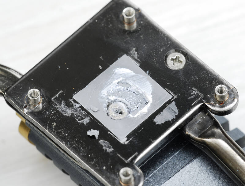
Now remove cooling solution and check...
Contact area of motherboard heatsink is not as good as expected to be, mount screw placed just above NF200 die. First time I saw such a "solution" on high-end motherboard
Software and firmware
BIOS shots of Gigabyte and ASUS boards. ASUS used UEFI for their latest P67 boards, while GBT still use legacy well-learnt Award.
UD7:
P67A-UD7 can be controlled under proprietary EasyTune6 tool, which is as usual is not easy at all in real-life overclocking. It does not work well with all bios versions, have overwhelmed design, but lack of necessary functionality, like system voltage monitoring and controls. Controls are laggy. Pity, such issues are common for "uber-super-overclocking tools" shipped with modern motherboards. Why not to create really simple and working tool, like SetFSB/CPU-Z/Rivatuner with simple interface w/o heavy graphics, just to do the job needed, fast and easy?..
M4E:
Maximus have similar overclocking tool too, but this one not as laggy, just need better usability, for example to have all settings on one screen section, not that countless folders in folders in submenus with only two-three settings in each
Benchmarking
Tier 1 : The Beginning
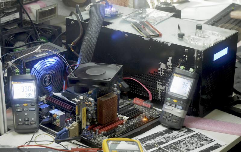
First to do - assemble test system and check if everything run smoothly and stable.
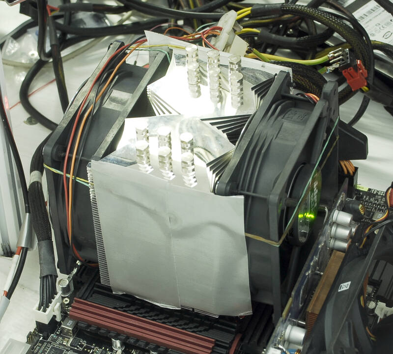
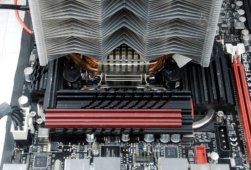
Start from CPU cooler install.
Clearance check for not the biggest cooling solution - Scythe Yasya in horizontal position.
On both boards cooler block nearest to CPU socket memory slot for any module with high heatsinks.
Even Dominator GT installed to second slot from socket with their accurate heatsinks was very close to touching
CPU cooler on ASUS board, and failed to fit with Gigabyte P67A-UD7.
Almost touched.
Fail to fit.
Of course it's not only motherboard design issue, but rather memory vendor stuff. Nice fancy heatsinks on
DDR3 stick are not for cooling, but for cool looking. Power output is so low for modern memory that it's not an issue
at all. And most extreme guys who cool memory to subzero are anyway don't care about awesomeness of stock
heatsinks on memory.
After assemble both boards boot and fully functional. Gigabyte P67A-UD7 had some issues with
Gigabyte PSU, I tried to use Odin GT 550W for some preliminary use, but board didn't even power on. Instant
shutdown when I press Power button. System doesn't power on even with everything disconnected.
Same PSU works okay with rest of my rigs, including Gigabyte P965-DQ6, ASUS P6T6, Maximus IV Extreme.
Maybe it's just exact PSU/mobo combo issue, but it was fun to have GBT PSU not working with GBT board.
2nd test - monitoring accuracy for voltages
Interesting part here. I will check all the voltages with Fluke 87V DMM and compare that to BIOS/Software
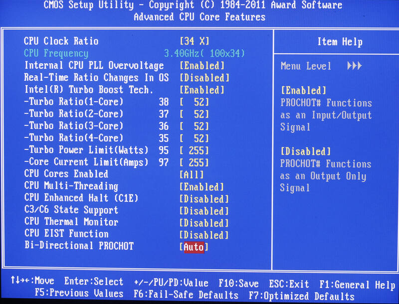
monitoring readout. For both boards I've set next settings from BIOS setup:
ASUS M4E - BIOS version 0676 x64 from 01/07/2011, EC: GMEB-0020, ME: 7.0.1.1141
Gigabyte UD7 - BIOS version F7a from 01/07/2011BCLK/PCIE Frequency: 100.3
Turbo Ratio: 52
Internal PLL Overvoltage: EN
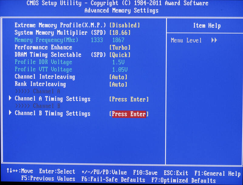
Memory Frequency: DDR3-1857MHz
EPU: Disabled
CPU Manual Voltage: 1.500
DRAM Voltage: 1.65V
Rest voltages left Auto
Spread Spectrum: DIS
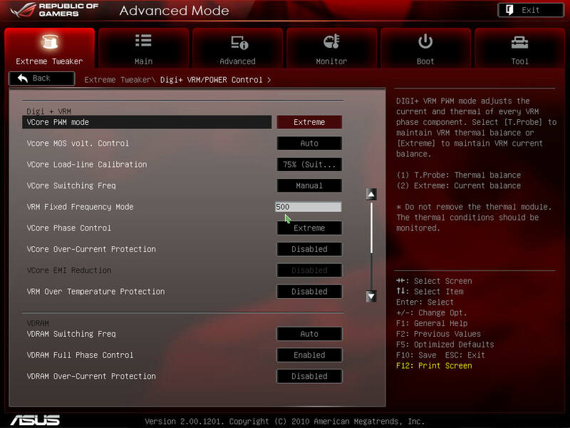
Digi+ VRM Control:
Vcore PWM mode: Extreme
Vcore MOS volt. Control: Auto
Vcore LLC: 75%
Vcore Freq: Manual, 500kHz
Vcore Phase control: Extreme
Vcore OCP: DIS
VRM OTP: DIS
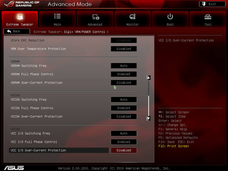
Rest convertor settings left Auto, Full Phase Control everywhere set EN
CPU settings:
Ratio: 34
Intel TM: DIS
HT: EN
Active cores: ALL
SpeedStep Tech: EN
Turbo: EN
C1E, C3 Report, C6 Report: DIS
All onboard devices disabled.
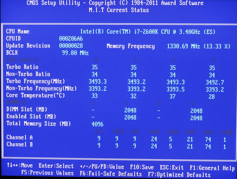
CPU Vcore monitoringBCLK/DMI/PCIE Frequency: 100.3 MHz
Turbo Ratio: 52
Internal PLL Overvoltage: EN
Memory Frequency (SPD multiplier): DDR3-1857MHz (16.00)
EPU: Disabled
CPU Manual Voltage: 1.500
DRAM Voltage: 1.65V
Rest voltages left Auto
Spread Spectrum: DIS
Digi+ VRM Control:
Vcore PWM mode: Extreme
Vcore MOS volt. Control: Auto
Vcore LLC: Level 1
Vcore Freq: Manual, 500kHz
Vcore Phase control: Extreme
Vcore OCP: DIS
VRM OTP: DIS
Rest convertor settings left Auto, Full Phase Control everywhere set EN
CPU settings:
Ratio: 34
Intel TM: DIS
Turbo Power Limit (Watts) - 255
Core Current Limit (Amps) - 255
HT: EN
EIST: DIS
Active cores: ALL
SpeedStep Tech: EN
Turbo: EN
C1E, C3 Report, C6 Report: DIS
All onboard devices disabled.
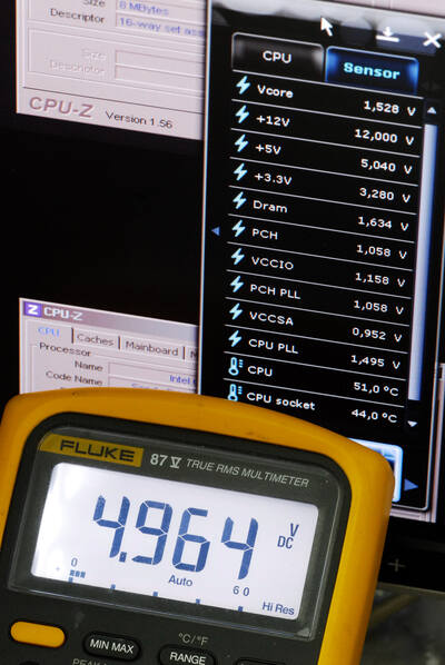
Min, max and average value during idle and one cycle of SPI,wPrime,Vantage CPU and Aquamark tests according to meter.
ASUS board
LLC 75%
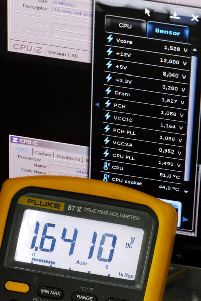
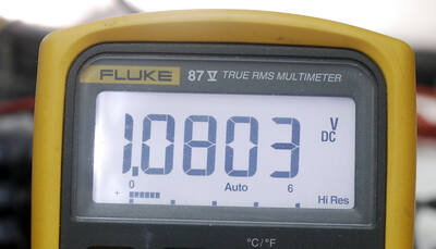
Average voltage photo, 1.5065V
Maximum voltage photo, 1.5083V
Minimum voltage photo, 1.5029V
Less than 10mV delta from min to max. Nice results and precise setting.
LLC 100%
Average voltage photo, 1.5661V
Maximum voltage photo, 1.5761V
Minimum voltage photo, 1.5606V
So max delta is about 15mV, and total voltage level is steady 60mV above BIOS 1.500 setting.
Gigabyte board
LLC Level 2
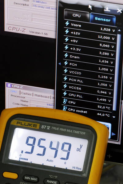
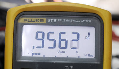
Average voltage photo, 1.5608V
Maximum voltage photo, 1.5988V
Minimum voltage photo, 1.5523V
46.5mV delta from low load to high load. Average level is 56mV above BIOS settings, topping at almost 1.6V.
LLC Level 1
Average voltage photo, 1.4982V
Maximum voltage photo, 1.5125V
Minimum voltage photo, 1.4749V
37mV delta, average level is quite near 1.500 V setting in BIOS.
So quite stable operation under heavy transitions from idle to 8-threaded wPrime/Vantage, I must admit.
Then monitoring rest of voltages
Main power supply rails monitoring:
+3.3, +5, +12V, measured on 24-pin ATX input power connector. Monitoring accuracy is okay for general use,
deviation is near +1%.
Rest system voltages working similar, with 1-2% accuracy. Could be better, but still these values are okay for
most users who are interested to see accurate voltages.
CPU PLL
DRAM Voltage
PCH Voltage
PCH PLL Voltage
CPU VIO voltage
System Agent voltage
Gigabyte board does not provide complete monitoring for user, so I'll just show BIOS settings and measured applied voltages.
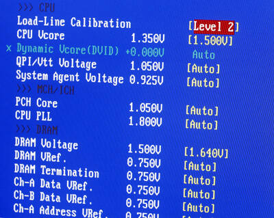
BIOS settings:
DRAM Voltage
VIO Voltage
System Agent voltage
Tier 2 : Overclocking Sandy Bridge
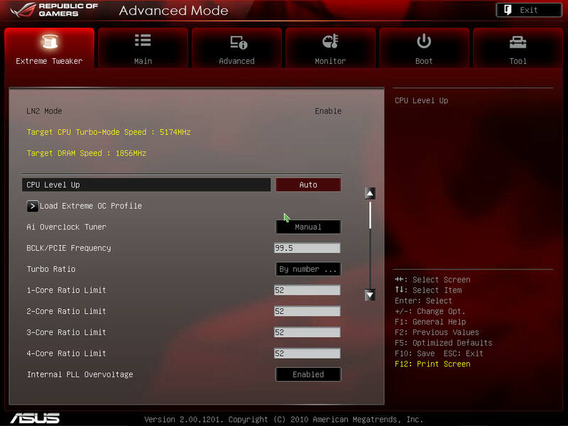
Lets check some BCLK clocking with reduced VCC to 1.45v and multi set to 48.
Tier 3 : Power stress test (thermals)
Maximus IV Extreme off, just on standby power, with CPU heatsink installed. NEC USB Bridge and peripheral controllers
heat up to mid-40's Celsius.
Power on at 5.17GHz 1.5V. System begin to heat up. wPrime 32M started
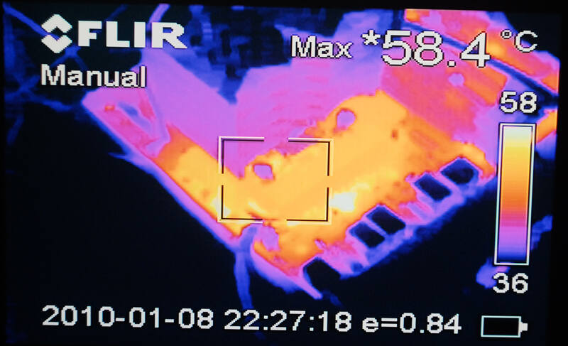
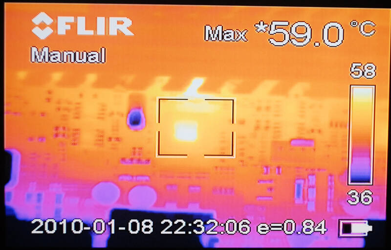
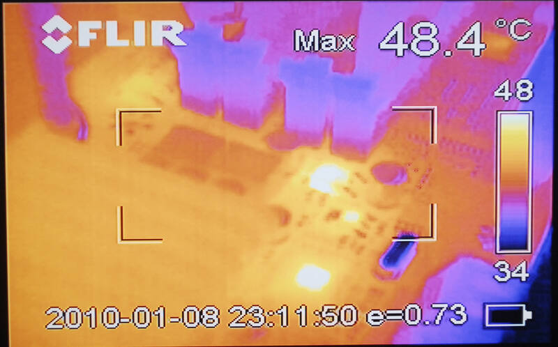
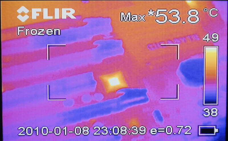
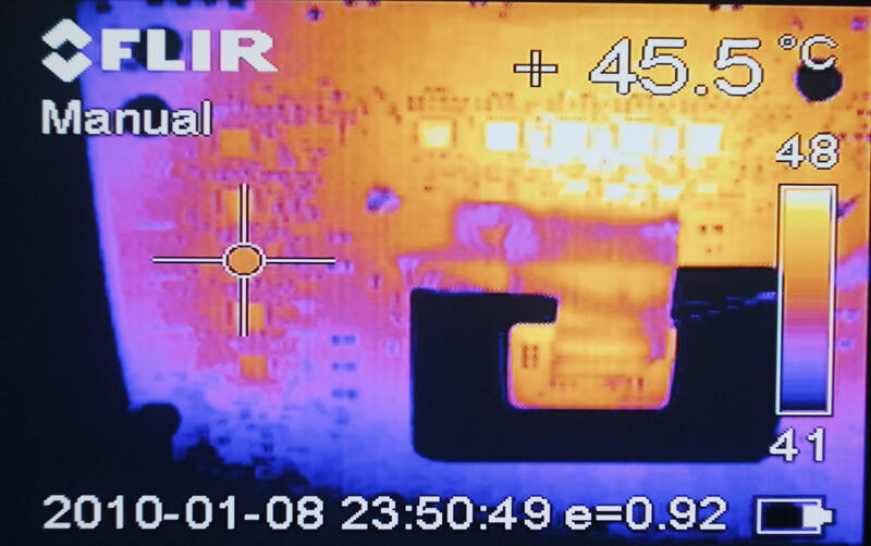
Thermal. With almost 5.2GHz Sandy Bridge quad core, heatsink on VRM module was in range 45 to 60C without any air-cooling
except stock low-speed fan on Scythe cooler.
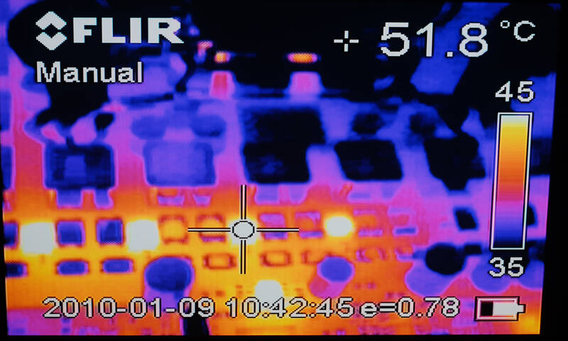
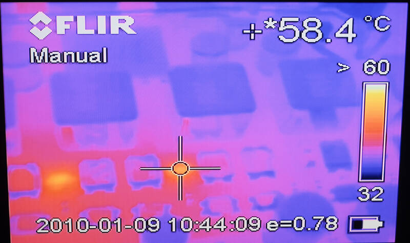
DC-DC convertor for USB 3.0 controllers run quite warm, above +60 C. This was always
the hottest point on motherboard during any tests and benchmarks.
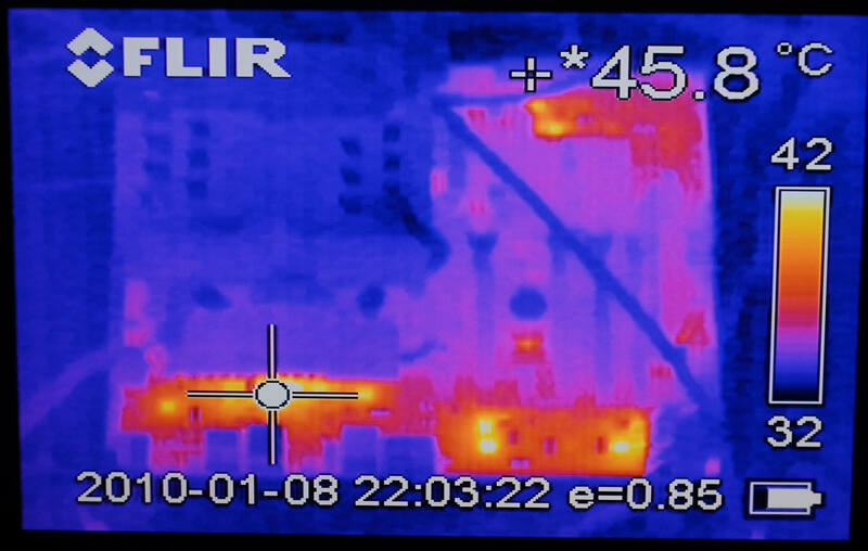
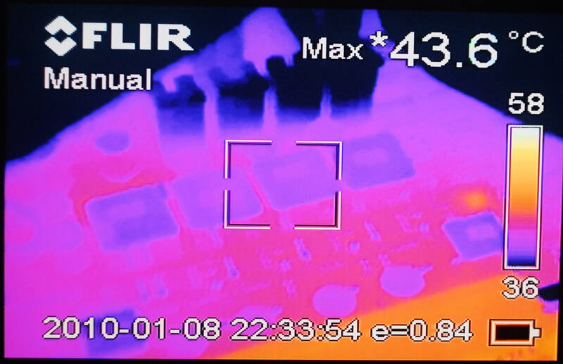
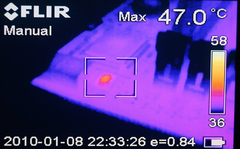
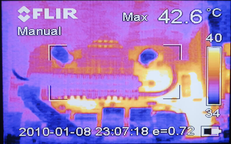
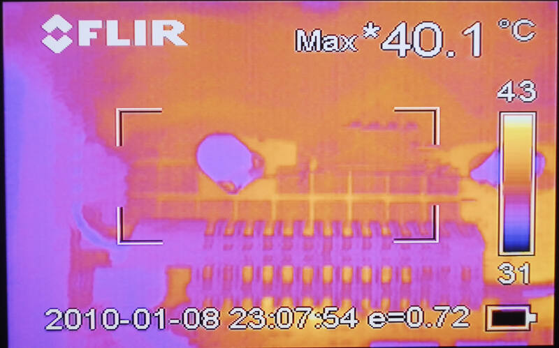
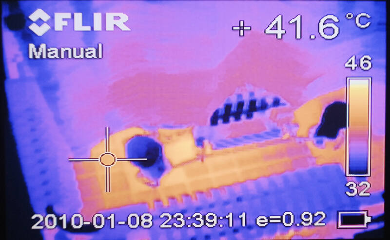
VDIMM power supply is dead cold, only +44. Maximum I saw during 2hrs of test - is 47 here.
IDT PCI-Express clock buffer near +50C, just 20 degrees about ambient.
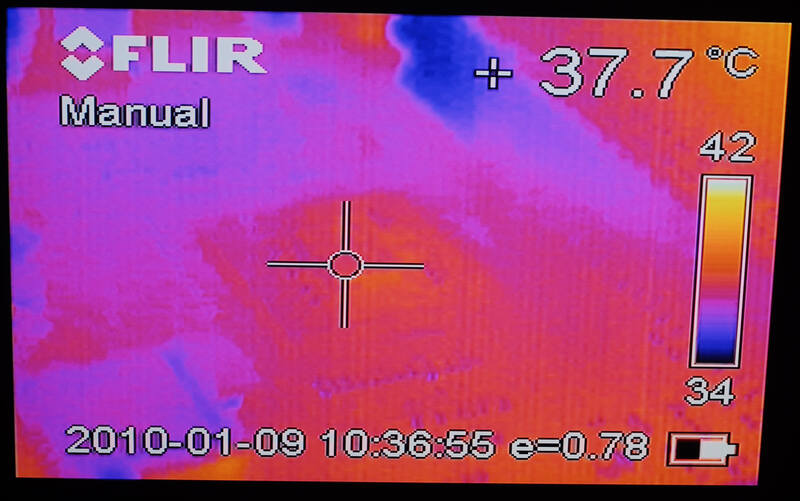
PCH runs near +50C, without any active airflow.
PLX switch working at +50-55C. Nothing except 8600GT card installed.
Super I/O area is cool, just a small chip which drives power-hungry LEDs in debug indicator heating up a bit.
NF200 bridge totally unpowered when not used. It's temperature is same as PCB, no heat at all.
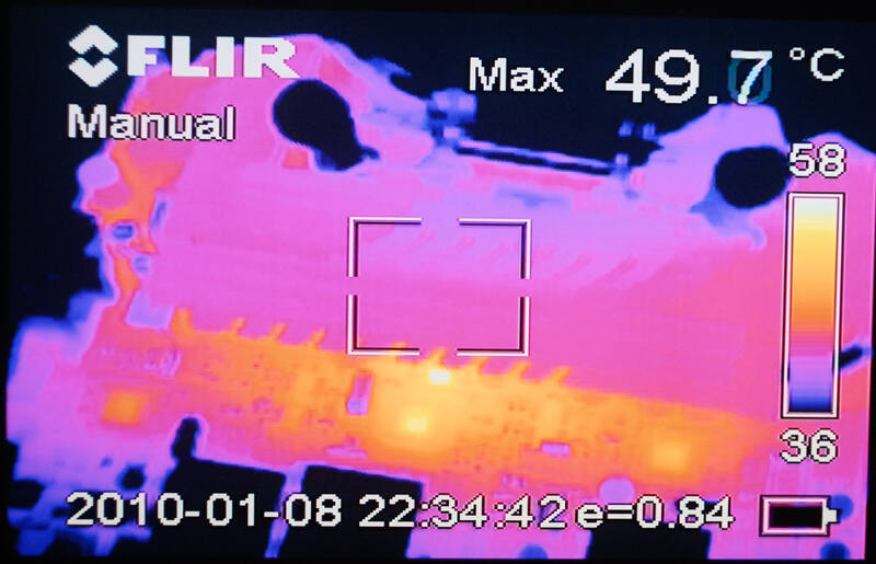
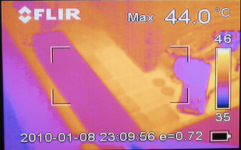
I was also interested in thermals without heatsink onboard, so decreased clock to 4.5GHz and voltage to 1.35V,
just to be safe.
Idle - 50-55c for drivers, even less for mosfets. MOSFETs on center was covered with matte paste, to
get rid from metal can reflectivity. Thermal imager accurate only on non-reflective surfaces.
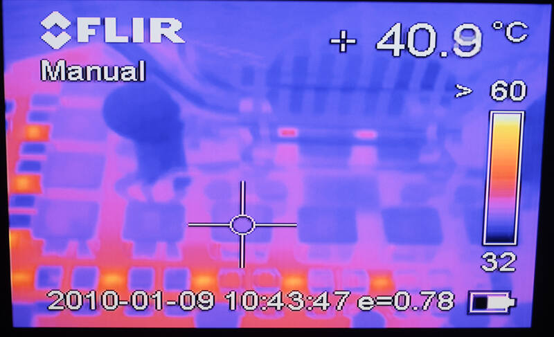
Coils run near 40-45C with 4.5GHz tests.
Drivers produced most part of heat, running near +60C.
Noise and transient testing
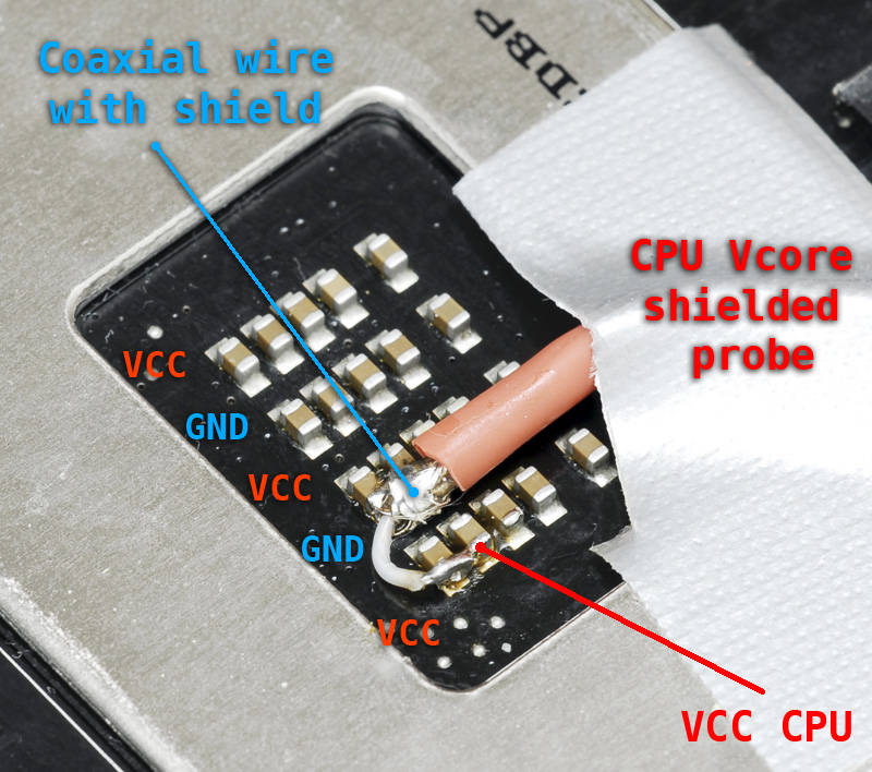
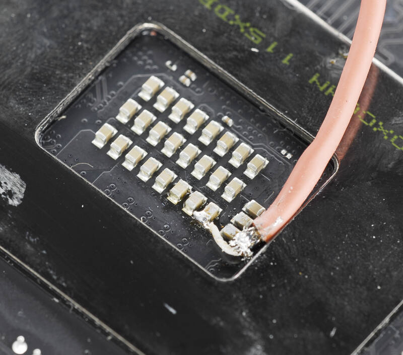
ASUS Vcore probe connect
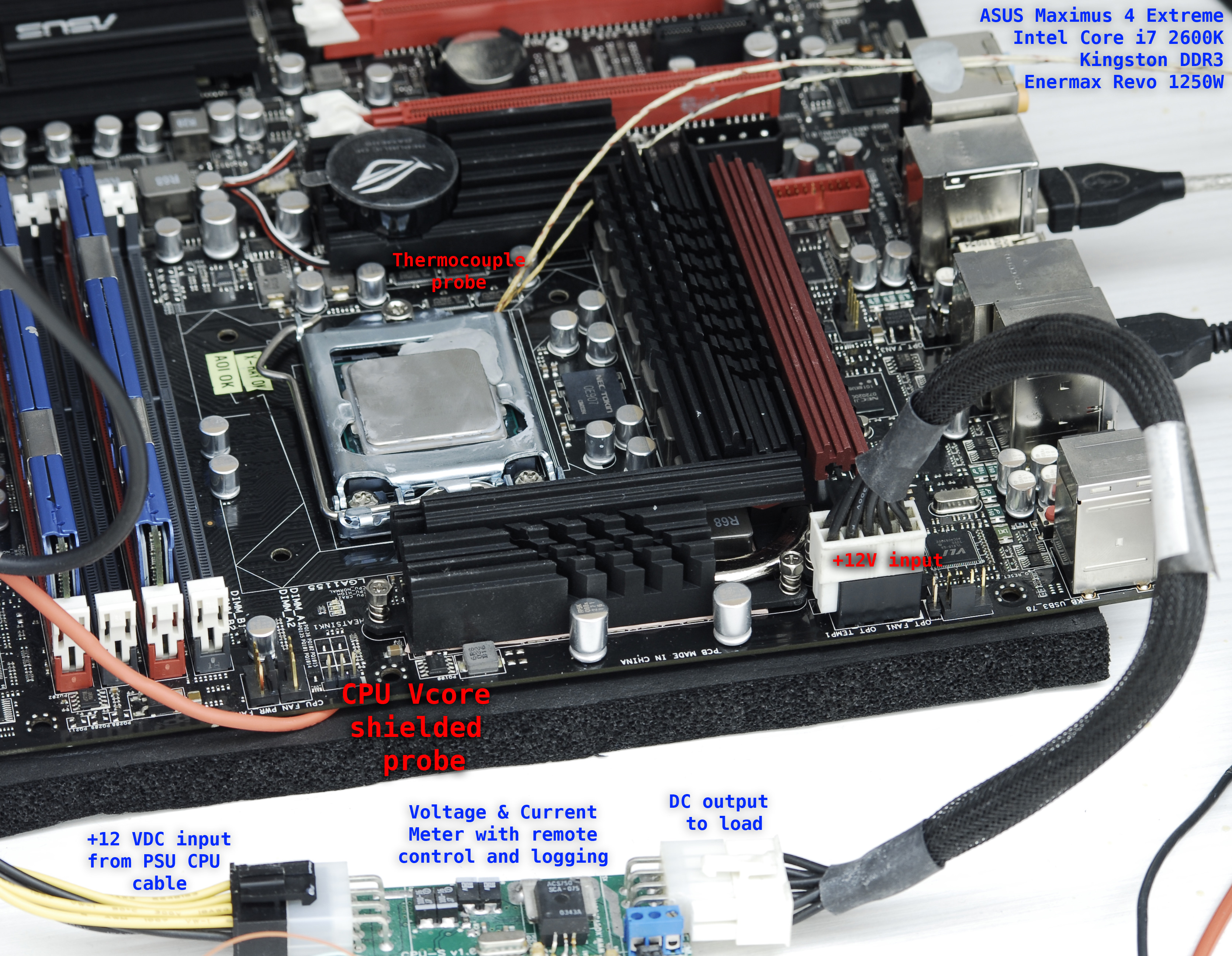
Shield of probe was connected to ground terminal to nearest capacitor in CPU cavity on back of motherboard, signal is VCCP terminal. For each tests below CPU was overclocked to 5.15GHz with 1.500 Vcore BIOS setting.
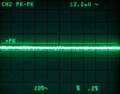
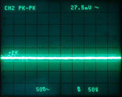
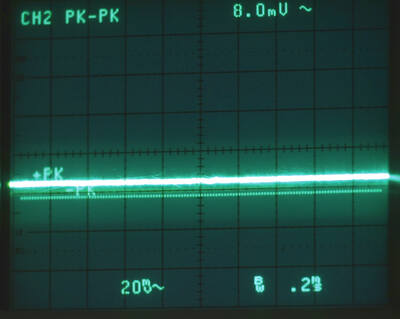
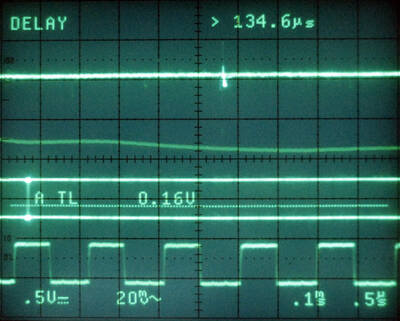
OS booted, system idle. 10-15mV range small noise, totally acceptable.
Light, SuperPI loading to CPU, noise increased to ~20mV, not noticeable actually.
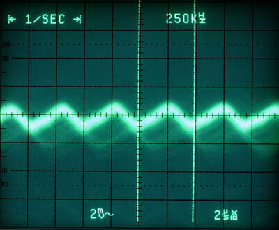
Small spike at running frequency of VRM, 500 kHz, observed.
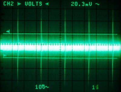
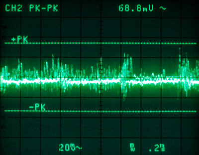
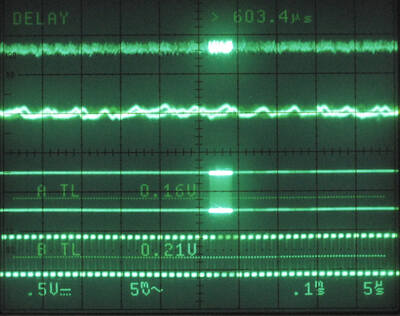
WPriming at 8 threads shows some increased ripple, 60-70mV max. It's okay for CPU.
wPrime at 5GHz and 1024 test (clock is limited by thermals with air-cooling), 65-75mV range. Okay too.
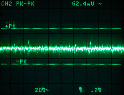
During Vantage CPU test VCCP is surprisingly clean, only ~30mV pk-pk ripple.
3Dmark03 test Nature, with 8600GT card on stock clocks. below 30mV range noise.
3Dmark03 test, with 480GTX on stock clocks. Never saw above 90mV.
In conclusion for CPU VRM on Maximus IV Extreme - it doing job very good. Run hotter than Gigabyte monster, but power quality is clearly better.
Overall YouTube video with M4E under noise tests:
Youtube demo during ASUS VRM testing
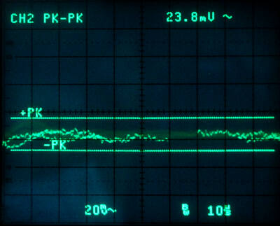
Gigabyte Vcore probe connect
Idle, booted OS, nothing loads system
Quite and safe.
Light load with 5.17GHz 1.5V in BIOS, LLC lvl 1.
Some 250kHz low-amplitude noise. About 10mV peak-peak.
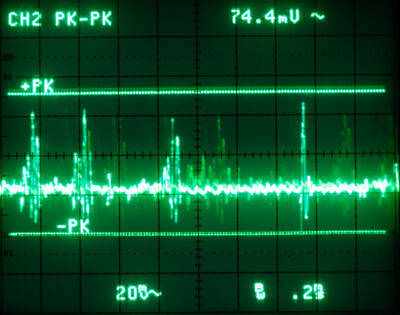
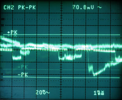
3D06 run thru CPU tests.
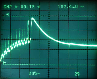
Whole bunch of oscillations happen. Average peak-peak level is 30-70mV
..with frequencies 22, 900Hz, few kHz.
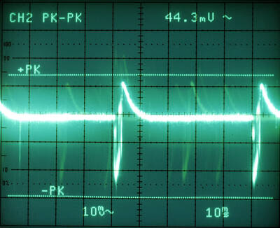
With medium to high-loads there are slow and big transients. 100-115mV peak-peak.
1MHz PWM1 signal added.
SuperPI 1M
Thermal shots
Applied stand-by power. System not working.
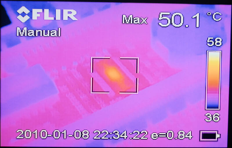
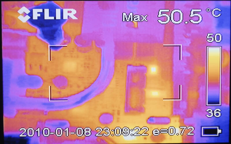
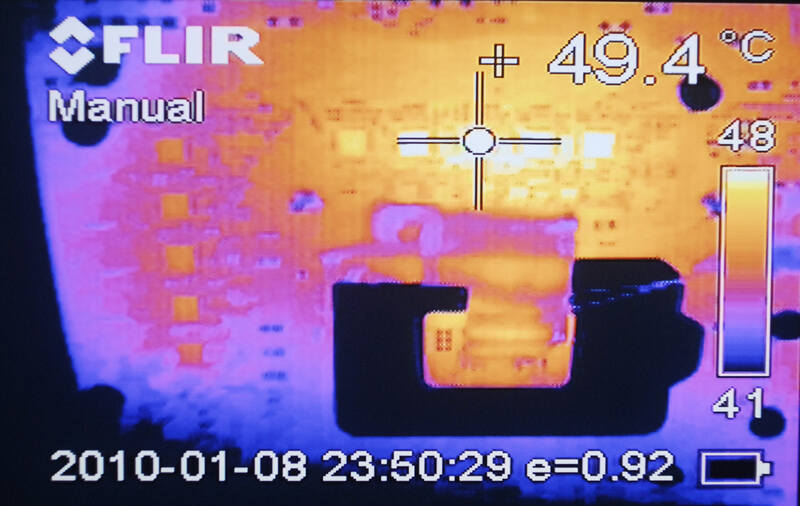
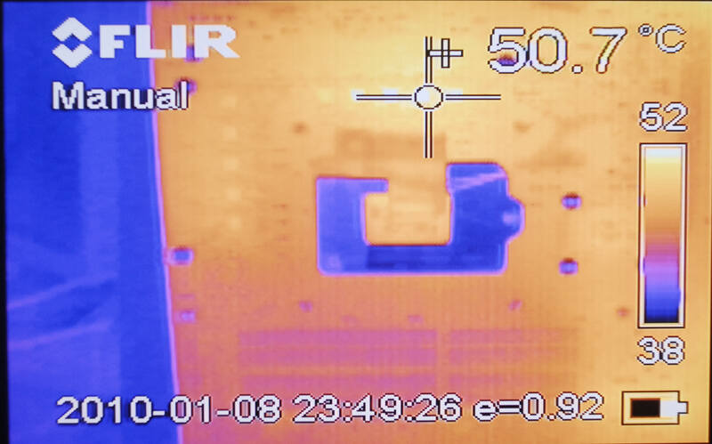
Starting system at 5.15GHz 1.5Vcore in BIOS. There is little choke temperature gradient.
Same USB 3.0 heat generated even in stand-by.
CPU auxilary power convertor run at about +50°C
ITE PCI hub comforts at 50-55 C
Main VRM chokes topped at +45°C during tests.
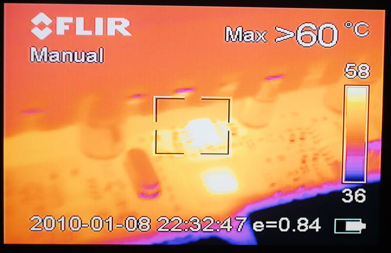
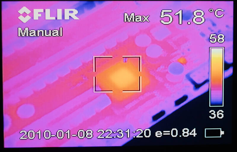
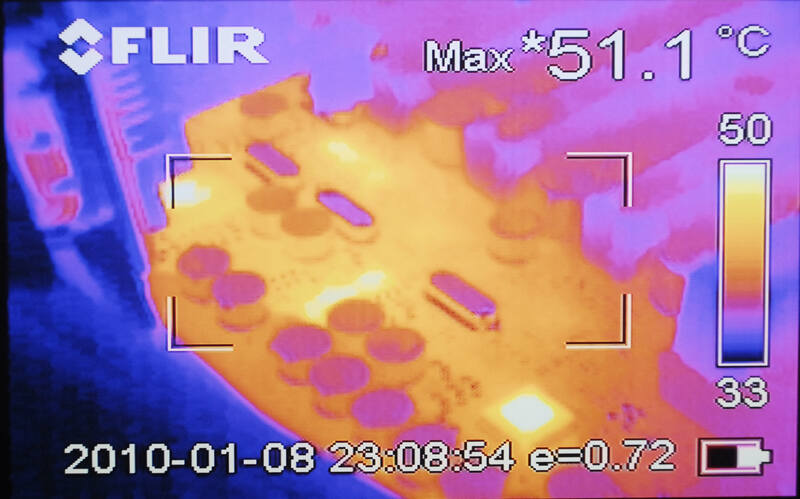
Back side of PCB is more interesting.
Top row of DMOS was about +5-7 °C warmer than left side.
Looks like current not balanced equally, but can be also just less copper on plane in that area.
Left DMOS chips.
Max temperature registered for bottom non-cooled DMOS-es was about +55-57°C
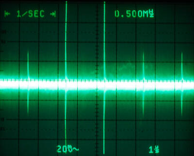
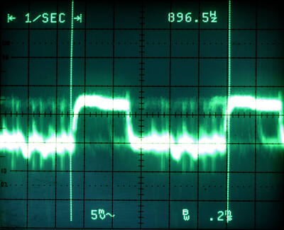
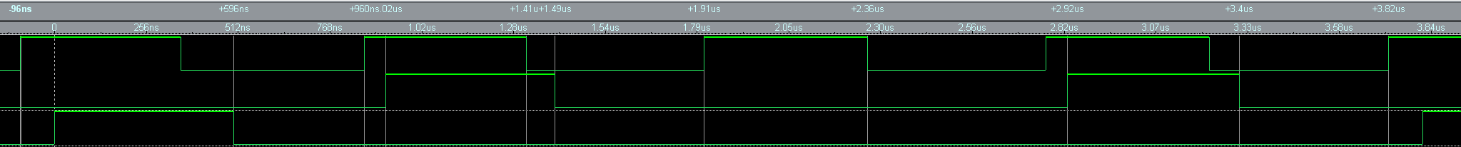
Actual phase PWM1 captured signals, Intersil output (top signal), After divider 1 stage (middle, 1/2 of clockrate, with 60ns delay, and after two divider stages (bottom signal, 1/4 frequency, 100ns delay)
So each divider adds noticeable delays to phase control signals. This mean that situation when more than one phase per moment can be firing, possibly raising noise level.
This waveform was captured using logic analyzer sampling at 250MHz rate.
Youtube demo during Gigabyte UD7 VRM testing
Power tests
-TBD Later-
Tier 4 : Extreme test
I didn't managed yet to gain any overclock increase with phase-change unit, with CPU evaporator temperature in range -40 to -20°C. But running Sandy on subzero allows overclockers to have sucessful benchmarking on heavyload tests, like Vantage CPU, 3D11, wPrime, etc. Most SB chips able to run 5.5+GHz SPI on water/air are overheating easily on heavy tests, so subzero helps to keep safe temperature, allowing to run test, no matter of no much scaling of freqencies themself. This is bit different approach on new platform, if you compare to LGA1366/1155/775 OC.
Test results
UD7 F7a bios VS MIVE 0088 bios
MIVE
UD7
Same rig, same cooling, same volts, same everything except mboard.
Full specs:
i7 2600K ES D1
Scythe HDT cooler
2x2G Kingston DDR3
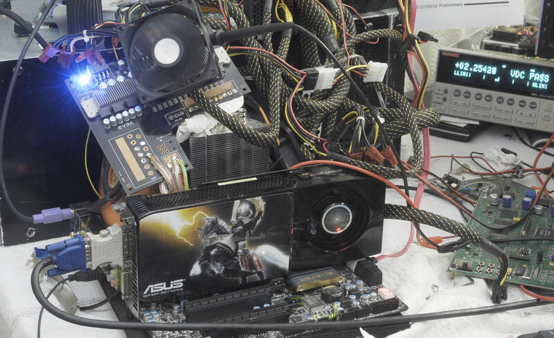
Single EVGA GeForce GTX 285 2GB with ASUS cooler and EVGA Untouchable for Vmem.
Enermax Revolution 1250+
Same Windows XP 32bit for both tests.
Lod 1.9 for all tests except nature, 4.9 for nature.
I forgot to enable HT but it should be not an influence so much.
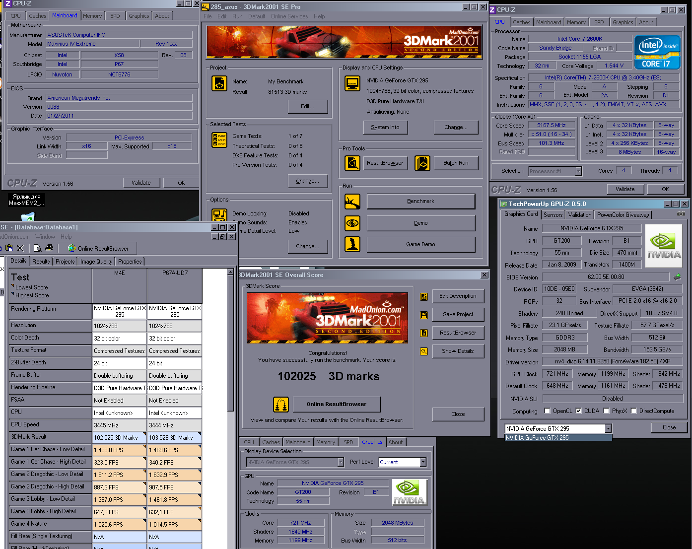
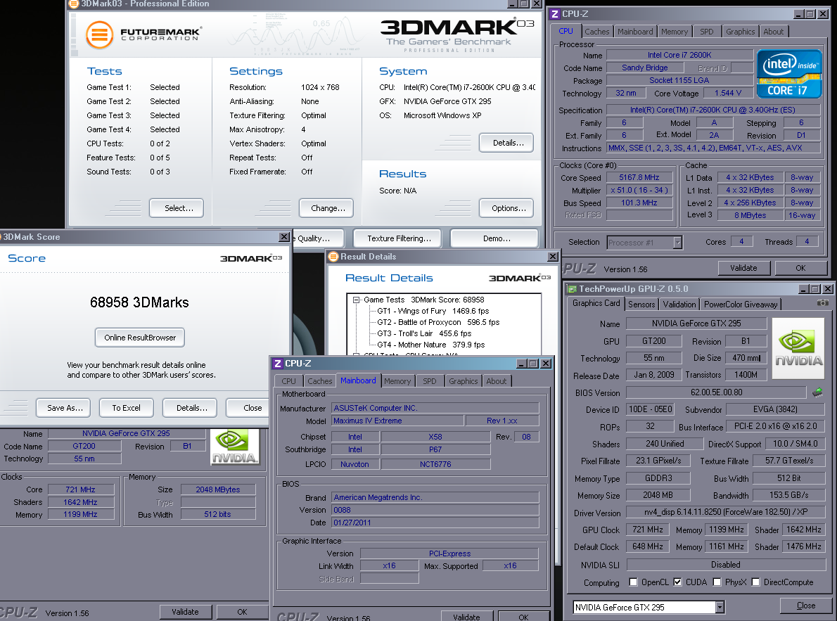
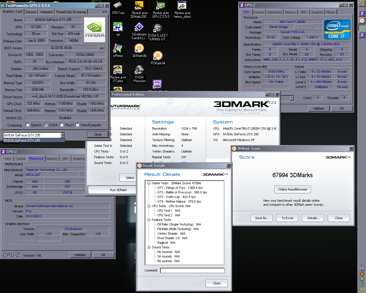
3DMARK03 (MIVE, 2600K D1 ES, 5167MHz air, EVGA GTX 285 2GB, 2x2G Kingston DDR3, Enermax 1250W)
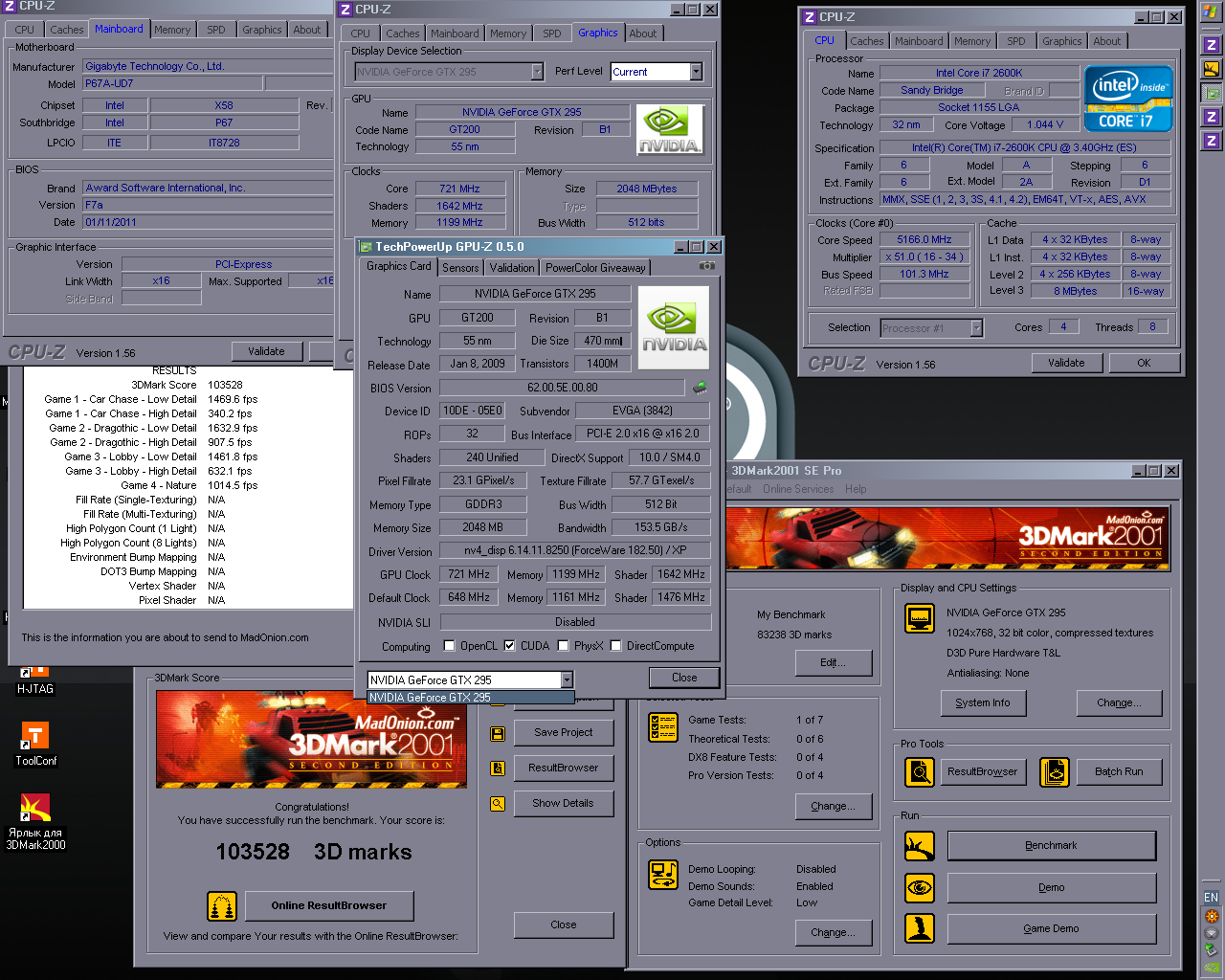
3DMARK03 (UD7, 2600K D1 ES, 5167MHz air, EVGA GTX 285 2GB, 2x2G Kingston DDR3, Enermax 1250W)
Multi-GPU scaling on MIVE
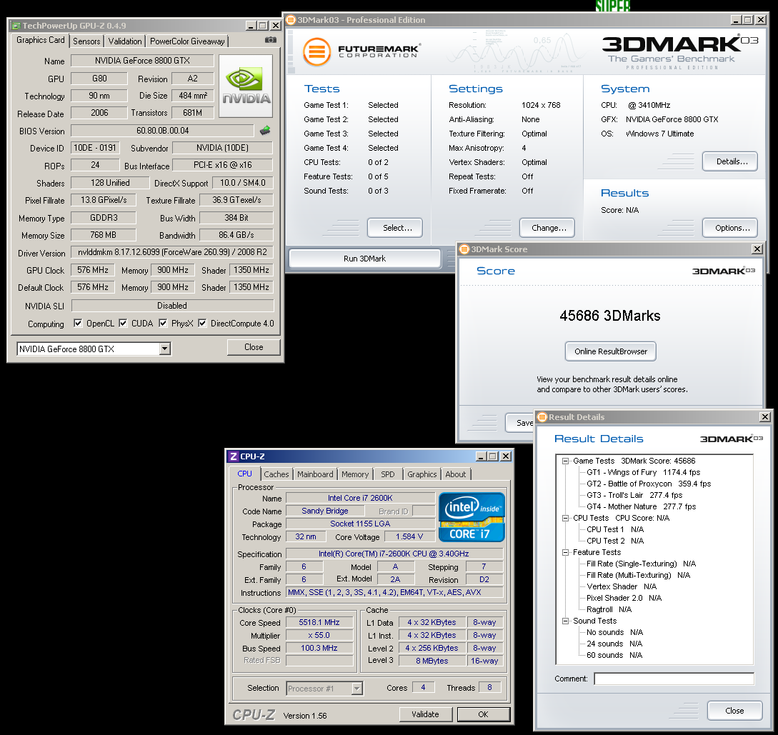
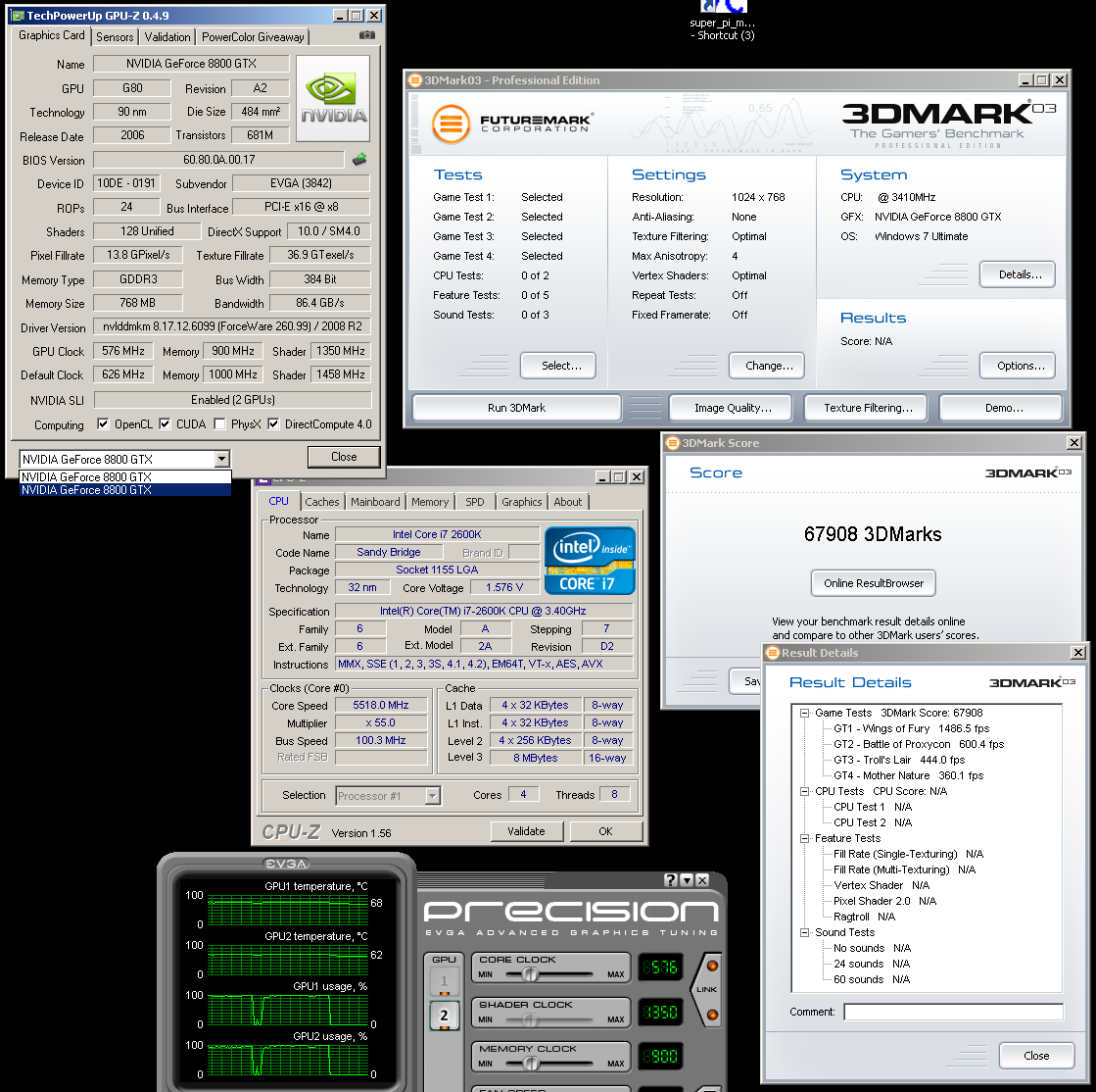
3DMARK03 (MIVE, 2600K D2, 5518Hz LS, 2x2G Kingston DDR3, Enermax 1250W)
Single 8800GTX - 45686
Two 8800GTX SLI thru NF200 - 67908
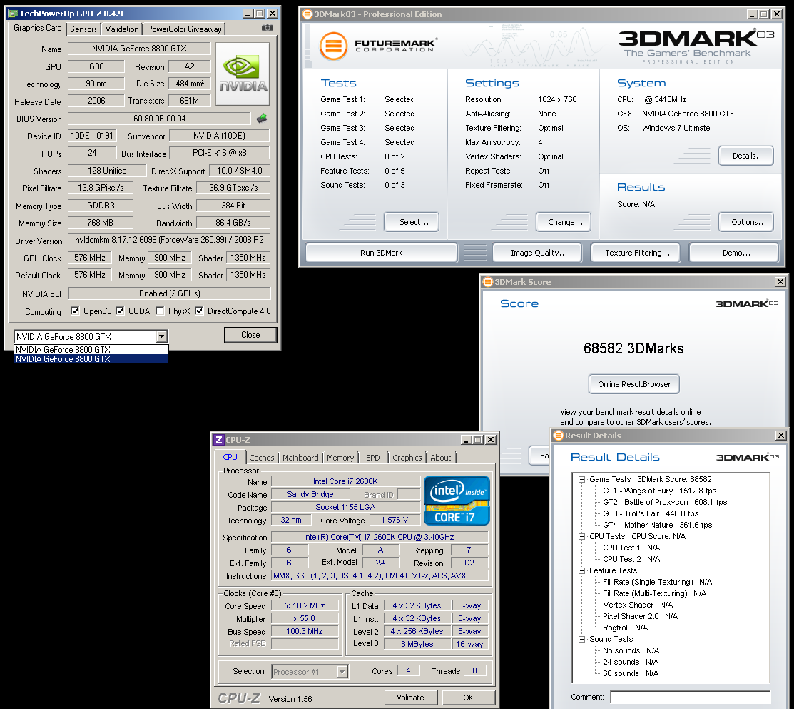
Two 8800GTX SLI by native SB lane split x8+x8 - 68582
So if you run 2-way it's wise to try avoiding NF200 bridge to reduce latency and have little better performance. All three tests with MIVE, coz UD7 don't allow have NF200 away if I recall correct
Aquamark comparsion
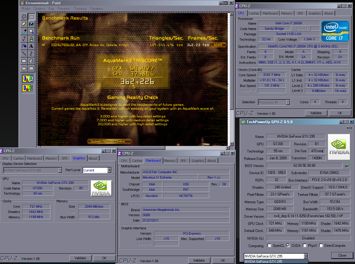
Aqua (MIVE, 2600K D1 ES, 5167MHz air, EVGA 285 GTX 2GB, 2x2G DDR3, Enermax 1250W)
362226, MIVE
LOD 4.9
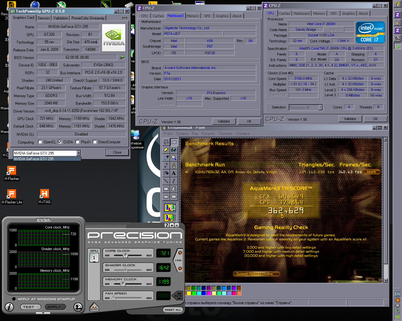
362629, UD7
LOD 4.9
Aquamark perf is about the same, in range of accuracy tolerance.
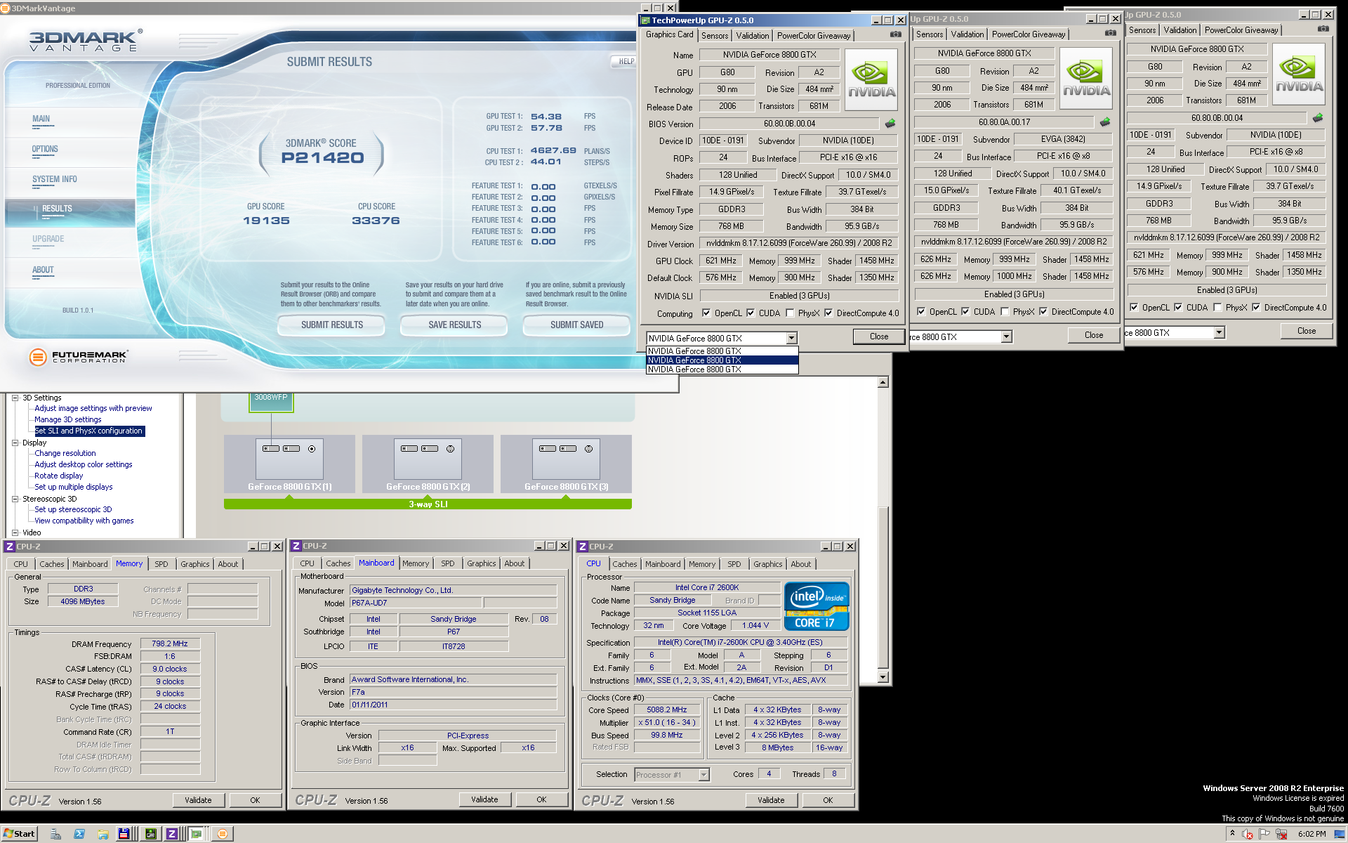
3-way 8800GTX on UD7 with Vantage
I tried to make 3-way SLI with 8800GTX on MIVE, but no luck. It was enabling only 2-way between 1st and 2nd card, or between 1st and 3rd card.
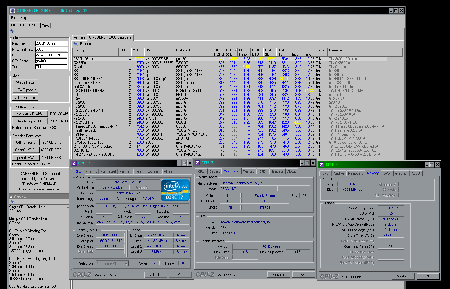
Btw, was discovered my old Cinebench 2003 tests from 2005 year "w00t"
Compare the evolution
From celeron 326 up to 2600K
Conclusion
ASUS ROG board and Gigabyte UD7 for Sandy Bridge processors marketed at same level as current flagship motherboard, but in real battle for benchmarks and usability ASUS solution looks like quite ahead. To be honest, I'm not an ASUS fan, but this time their solution works better for me
Actual practial comparsion of both boards in VRM performance side allow to see, that boards run similar, UD7 have overvolts more with similar LLC settings, have more noise on plane, but VRM runs cooler in general. ASUS board run have better voltage precision, much more VRM adjustable settings thru BIOS, wider voltage range. bit warmer.
I could not see any practical sense to make 24-phase VRM for LGA1155 platform. Yes, it sounds cool, but it's not the key necessary for overclocker (and never was). What is essential for overclockers - is ability to control everything, solid and stable overclocking software, useful and clear BIOS settings, and minimum of issues. Good 6/8-phase design still able to deliver necessary power, and practice shows that even Intel DP67BG is able to make 5.5GHz Sandy Bridge happiness, not matter of it's "weak" VRM.
We should wait for new revisions of Sandy Bridge boards to make final statement, but even current models able to reach much more than 5000MHz using just normal air cooler, without any subzero madness, which is just cool. I'm sure about new world records using Sandy Bridge platform, just after people learn new platform a bit.
Credits:
* cyclone for hardware and support
* Peter for great support and cooperation
* k|ngp|n for doing amazing things constantly
* And many many others who put effort to OC :\:\:\:\:\
Stay tuned, keep following. TiN


 Reply With Quote
 Saaya yupp, I agree


 )
)


Bookmarks