

Some other thing is more weird and surprising:Originally Posted by Voodoo²

http://semiaccurate.com/forums/showp...5&postcount=13
A1 chips production underwayed in September? wtf?stepping A1, week 36, year 2011.


Some other thing is more weird and surprising:
http://semiaccurate.com/forums/showp...5&postcount=13
A1 chips production underwayed in September? wtf?stepping A1, week 36, year 2011.
I´m not sure what "FA1" stands for but as long as I remember the steppings always were indicated by one of the letters here "FD8150FRW8KGU". For Example:
Phenom II X4 955 C2 stepping HDZ955FBK4DGI
Phenom II X4 955 C3 stepping HDZ955FBK4DGM
Last edited by Voodoo²; 10-05-2011 at 11:01 AM.
ASUS M4A79T Deluxe
Phenom II X2 555 BE (4 cores unlocked)
Sapphire 6770 1GB
G.Skill RipJaws 2 x 2GB 1600MHZ cl7
480 watt Topower/Tagan Power supply
Thermaltake Soprano
24" 1920x1080 BenQ G2410HD
MAXTOR 500GB 32MB x2
BenQ DW1650 16x Dvd burner
Dang, I wish I have one before Retail Launch !!!
Gaming Rig
CPU : AMD Ryzen 7 3700X (45W ECO mode)
HSF : Noctua C14S
MB : ASRock X470 Taichi Ultimate
RAM : G.Skill F4-3000C14-16GTZR x4 @ DDR4-3000 CL14
VGA : MSI RTX2070
PSU : Antec NeoECO Gold 650W
Case : Corsair 100R ATX
SSD : Samsung PM981a 1TB + Corsair MP510 1.9GB M.2 SSD
A1 is not the stepping unless they changed the naming scheme...
CACDC for Deneb translates FA1 on these new processors...
Smile
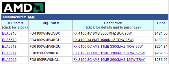
whats the difference between box and try? the 4100 for 121$ sounds very desirable. but just seems a little strange looking
2500k @ 4900mhz - Asus Maxiums IV Gene Z - Swiftech Apogee LP
GTX 680 @ +170 (1267mhz) / +300 (3305mhz) - EK 680 FC EN/Acteal
Swiftech MCR320 Drive @ 1300rpms - 3x GT 1850s @ 1150rpms
XS Build Log for: My Latest Custom Case
Someone guess it's a copy-paste typo.
http://www.planet3dnow.de/vbulletin/...&postcount=625
Last edited by undone; 10-05-2011 at 12:09 PM.
yeah i was expecting something like that. the 189$ should be 4C, and the 121$ should be an x4 non FX model cpu, for it all to make sense
2500k @ 4900mhz - Asus Maxiums IV Gene Z - Swiftech Apogee LP
GTX 680 @ +170 (1267mhz) / +300 (3305mhz) - EK 680 FC EN/Acteal
Swiftech MCR320 Drive @ 1300rpms - 3x GT 1850s @ 1150rpms
XS Build Log for: My Latest Custom Case
I dont think that is real price. Its some kind of error.
But, difference between box and tray is cooler. Box has cooler with it, tray does not have cooler with it.
I get concerned when I see people touting review units that only include one chip.
there are 4 chips to review. if we get only one chip reviewed on the 12th I will be smashing things.
AMD said 80% more performance than single threaded (in the same module, also presuming same frequency), meaning 180% of single threaded, or (180/2) 90% for each core.
start smashing then, till now I only know about 8150 models being shipped in press kits...
Question : Why do some overclockers switch into d*ckmode when money is involved
Remark : They call me Pro AsusSaaya yupp, I agree
Actually they officially said (in presentations) 80% of CMP design which was presumably CMP-type Bulldozer with nothing shared(except maybe L3). But we have been over this before.
I suspect the biggest hit will be running fp heavy code and that the 80% figure comes from that. It's logical when you think about it : instead of replicating "full" cores in order to get 8 FPUs,you invest in each FPU more resources,increase the BW to the unit and make it shareable between 2 integer cores.In the process you make the unit in the way so that it uses SMT for 2 threads running on 2 dedicated pieces of hardware inside it. This way you have 4 new FPUs ,now shared, that produce only 25% less throughput than 8 "full" ones in CMP (without SMT probably) and all this saves you considerable die area and grants you some TDP and clock headroom. Pretty neat idea isn't it?
look at all those goodies that come with it
hmmm some got them early(scroll down to last part)
http://www.tipidpc.com/viewtopic.php...2787&page=4183
Last edited by duron; 10-05-2011 at 07:39 PM.
results anybody? nda?
plenty of press kits around, give us a tease
FX-8350(1249PGT) @ 4.7ghz 1.452v, Swiftech H220x
Asus Crosshair Formula 5 Am3+ bios v1703
G.skill Trident X (2x4gb) ~1200mhz @ 10-12-12-31-46-2T @ 1.66v
MSI 7950 TwinFrozr *1100/1500* Cat.14.9
OCZ ZX 850w psu
Lian-Li Lancool K62
Samsung 830 128g
2 x 1TB Samsung SpinpointF3, 2T Samsung
Win7 Home 64bit
My Rig
You know, I'm really excited that FX is so close now....
Reguardless of final performance compared to Intel, I can't help but think that once we get our hands on these
chips all the crazy fud/benchies are going to seem ridiculous....
I've been reading all this stuff for the last 9 months, and you wouldn't believe how bad I've been biting my tounge.
Some may have been right, some may have been wrong, but once I (we) can test for ourselves all the questions will finally be answered!
I'm sure there's some Firmware/Software/Hardware/OS tweaks that need to be done to get the best results from this new uARCH, but at least
it will finally be out there and worked on.
BRING'EM ON BABY.....
If nothing else, I need a new adventure, and this chip looks like fun!
Last edited by Daveburt714; 10-05-2011 at 09:57 PM.
AMD FX-8350 (1237 PGN) | Asus Crosshair V Formula (bios 1703) | G.Skill 2133 CL9 @ 2230 9-11-10 | Sapphire HD 6870 | Samsung 830 128Gb SSD / 2 WD 1Tb Black SATA3 storage | Corsair TX750 PSU
Watercooled ST 120.3 & TC 120.1 / MCP35X XSPC Top / Apogee HD Block | WIN7 64 Bit HP | Corsair 800D Obsidian Case
First Computer: Commodore Vic 20 (circa 1981).
This architecture seems very voltage friendly as well
So is Llano, GF's 32nm is very voltage hungry...2v+ for CPU-Z validations on LN2/LHe with BD.
It will be fun
Smile
CMP (Chip Multi Processor) is two "full" cores, and CMT (Cluster-based MultiThreading) is what they call the modules idea:
That's the slide I was referencing, where they said 80% gain
Although in retrospect it also says 50% area investment, so I'm not sure if that exactly describes the actual BD modules used in Zambezi, which AMD said have 12% larger die area than a "full" core (hypothetical BD "full" core, not K10.5).
Bulldozer's FlexFP:
http://blogs.amd.com/work/2010/10/25/the-new-flex-fp/
Basically it is two 128-bit FMAC's with a shared scheduler, which works alongside two integer cores.
It looks like it almost has enough FP resources to get the same performance as two "full" cores, the exception being if two 256-bit instructions were issued at once - though the capability to do that requires much more (largely unused) die area.The Flex FP unit is built on two 128-bit FMAC units. The FMAC building blocks are quite robust on their own. Each FMAC can do an FMAC, FADD or a FMUL per cycle. When you compare that competitive solutions that can only do an FADD on their single FADD pipe or an FMUL on their single FMUL pipe, you start to see the power of the Flex FP – whether 128-bit or 256-bit, there is flexibility for your technical applications. With FMAC, the multiplication or addition commands don’t start to stack up like a standard FMUL or FADD; there is flexibility to handle either math on either unit. Here are some additional benefits:
- Non-destructive DEST via FMA4 support (which helps reduce register pressure)
- Higher accuracy (via elimination of intermediate round step)
- Can accommodate FMUL OR FADD ops (if an app is FADD limited, then both FMACs can do FADDs, etc), which is a huge benefit
The new AES instructions allow hardware to accelerate the large base of applications that use this type of standard encryption (FIPS 197). The “Bulldozer” Flex FP is able to execute these instructions, which operate on 16 Bytes at a time, at a rate of 1 per cycle, which provides 2X more bandwidth than current offerings.
By having a shared Flex FP the power budget for the processor is held down. This allows us to add more integer cores into the same power budget. By sharing FP resources (that are often idle in any given cycle) we can add more integer execution resources (which are more often busy with commands waiting in line). In fact, the Flex FP is designed to reduce its active idle power consumption to a mere 2% of its peak power consumption.
The Flex FP gives you the best of both worlds: performance where you need it yet smart enough to save power when you don’t need it.
The beauty of the Flex FP is that it is a single 256-bit FPU that is shared by two integer cores. With each cycle, either core can operate on 256 bits of parallel data via two 128-bit instructions or one 256-bit instruction, OR each of the integer cores can execute 128-bit commands simultaneously. This is not something hard coded in the BIOS or in the application; it can change with each processor cycle to meet the needs at that moment. When you consider that most of the time servers are executing integer commands, this means that if a set of FP commands need to be dispatched, there is probably a high likelihood that only one core needs to do this, so it has all 256-bit to schedule.
Floating point operations typically have longer latencies so their utilization is typically much lower; two threads are able to easily interleave with minimal performance impact. So the idea of sharing doesn’t necessarily present a dramatic trade-off because of the types of operations being handled.
Here are the 4 likely scenarios for each cycle:

So I would think two thread scaling (in one module) is largely a matter of the shared front-end's capability to feed the execution resources (as well as memory bandwidth, latencies etc which needs to be improved the more cores you have)
Last edited by Apokalipse; 10-05-2011 at 10:30 PM.
Only neat if you get more than 25% higher frequencies. I doubt that doubling the FPUs would make a big hit on frequencies. The FPUs count for a very small part of total die area so saving mm² isn't worth it. And I doubt higher power consumtion would would lower the frequencies much.
Doubling the FPU's takes massively more die area, meaning more power usage, and you can't clock it as high if you want to remain within a certain TDP.
Floating point units are much more complex than integer units, and take up much more die area.The FPUs count for a very small part of total die area
instruction sets like SSE, AVX use the FPU primarily.
Last edited by Apokalipse; 10-06-2011 at 12:01 AM.
@Apokalipse
The slide about cmt is from 2005,long before amd had any real HW im their hands. I stick with what they said at FAD 2010 and that's 80% of cmp design in less die area. The rest of the stuff you quoted is well known information and doesn't go against what I wrote. I even believe there won't be massive hit in integer throughput from running 2 threads on a module. Fp may see the best numbers if threads are 1st scheduled on different modules but this has to be verified.
@Boris
You do realize that in order to get 8 *full* fpus the old way, you have to replicate front ends ,integer exec. units and L1 and L2 caches ,right? This leaves you with wasted and doubled die area that will mostly sit idle (especially fp unit). Beaty of bulldozer is exactly in maximizing perf./watt/mm^2. Btw ,the most power hungry part of the core is usually fpu...
My point is that I don't think the FlexFP will much less performance than two conventional "full" 256-bit FPU's if the frontend can do its job and keep the execution resources fed.
I think the only case where it is limited in execution resources is if there are two 256-bit instructions from two threads at once, but that's a very rare case.
So yes it won't be as fast as two "full" cores. I'm just saying that I don't think available execution resources is the main reason for this (for either integer or FP). The FlexFP looks very efficient and much less transistor/die-area wasteful than two conventional 256-bit FPU's in two "full" cores.
The frontend is very much beefed up vs K10.5 though; which it has to be to feed the extra execution resources for two threads.
Last edited by Apokalipse; 10-06-2011 at 02:20 AM.
I am not against BD CMT design, but without stronger IPC it's just useless.
So with CMT we have 80% performance of a true core. But the problem is that it's not a 100% performance core + 80% CMT core( comparing Intel + HT), it's 80% performance for both cores in module so...
If we calculate 0.8(80%) * 8 = 6.4 so 6.4 true cores performance, so a bigh hit.
This desing it doesn't scale well the more cores you put.
If we put that the IPC isn't much better- may be the same, not to be pesimist to say lower, than wat we got?
A 6.4 cores with a 10% speed bump, may be a 6.8-7 true cores performance.
So what "maximizing perf./watt/mm^2" - not performance anyway,
I have my info, and BD it's a disappoiment. For an " 8core" . As it' price, overall performance is between 2500K and 2600K, and will be hoter on air cooling than SB.
Last edited by xdan; 10-06-2011 at 02:46 AM.
i5 2500K@ 4.5Ghz
Asrock P67 PRO3
P55 PRO & i5 750
http://valid.canardpc.com/show_oc.php?id=966385
239 BCKL validation on cold air
http://valid.canardpc.com/show_oc.php?id=966536
Almost 5hgz , air.
You sure ? got data to back that statement ?
Question : Why do some overclockers switch into d*ckmode when money is involved
Remark : They call me Pro Asus
You have a point, but I think Cinebench uses mostly scalar maths, utilizing only the 1/4 or 1/2 of the 128 bit wide engines (depending on that if it uses single or double precision).
Also, it doesn't use FMA, so the underlaying FADD and FMUL units in an FMAC never work at once (or at least only one execution starts, per cycle).
0.5 x 0.5 = 0.25 -> 1/4 FPU utilization/thread (with MT)
0.25 x 0.5 = 0.125 -> 1/8 FPU utilization/thread (with MT)
Of course, it's quite theoretical as the sharing of the FPU is not exactly 50% per thread per module all the time, and these are the peak values.
Depends on if FMA is utilized or not and that if only one or two threads run in a given module, I think. AFAIK the FADD and FMUL units in the K10 cores are capable of working (or starting/finishing) parallelly. With BD, with regular code you can't have the underlaying FADD and FMUL units utilized (or new execution started/finished) at once, in a given FMAC, unless you use FMA code. And you have only one FMAC per thread in case both threads needs them at once...
So, with a single-threaded (or one thread per module) regular code it will perform comparable to K10 (because the second FMAC can be utilized anytime), but if more than 4 threads are running scaling will be worse.
But, perhaps I'm wrong somewhere. Feel free to correct me, then.
Last edited by dess; 10-06-2011 at 03:05 AM.
 Posting Permissions


 Reply With Quote


Bookmarks