Results 1 to 16 of 16

Thread: Denser computer chips possible with plasmonic lenses that 'fly'

  1. #1
    Xtreme Enthusiast
    Join Date
    Oct 2006
    Location
    Austin, Texas
    Posts
    822

    Denser computer chips possible with plasmonic lenses that 'fly'

    BERKELEY — Engineers at the University of California, Berkeley, are reporting a new way of creating computer chips that could revitalize optical lithography, a patterning technique that dominates modern integrated circuits manufacturing.

    By combining metal lenses that focus light through the excitation of electrons - or plasmons - on the lens' surface with a "flying head" that resembles the stylus on the arm of an old-fashioned LP turntable and is similar to those used in hard disk drives, the researchers were able to create line patterns only 80 nanometers wide at speeds up to 12 meters per second, with the potential for higher resolution detail in the near future.

    "Utilizing this plasmonic nanolithography, we will be able to make current microprocessors more than 10 times smaller, but far more powerful," said Xiang Zhang, UC Berkeley professor of mechanical engineering and head of the research team behind this development. "This technology could also lead to ultra-high density disks that can hold 10 to 100 times more data than disks today."

    schematic of plasmonic lithography:


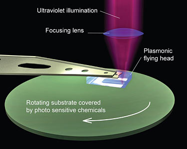
    In this schematic of plasmonic lithography, the plasmonic flying head produces nanoscale patterns onto the spinning disk covered with photo sensitive chemicals. Ultraviolet light is delivered through the flying head onto the plasmonic lenses, which are used as optical styluses in this process. The setup resembles a stylus playing a record on traditional LP turntables. (Liang Pan and Cheng Sun, UC Berkeley)

    Zhang worked jointly on the project with David Bogy, UC Berkeley professor of mechanical engineering. The study now appears online in Nature Nanotechnology, and is scheduled for the journal's December print issue.

    The process of optical lithography shares some of the same principles as film photography, which creates pictures by exposing film in a camera to light, and then developing the film with chemical solutions. In the semiconductor industry, optical lithography is a process in which light is transferred through a mask with the desired circuit pattern onto a photosensitive material, or photoresist, that reacts chemically when exposed. The material then goes through a series of chemical baths to etch the circuit design onto a wafer.

    "With optical lithography, or photolithography, you can instantly project a complex circuit design onto a silicon wafer," said Liang Pan, a UC Berkeley graduate student working with Zhang and Bogy, and one of three co-lead authors of the Nature Nanotechnology paper. "However, the resolution possible with this technique is limited by the fundamental nature of light. To get a smaller feature size, you must use shorter and shorter light wavelengths, which dramatically increases the cost of manufacturing. Also, light has a diffraction limit restricting how small it can be focused. Currently, the minimum feature size with conventional photolithography is about 35 nanometers, but our technique is capable of a much higher resolution at a relatively low cost."

    The UC Berkeley researchers chose a different approach to overcome the diffraction limit of light. They took advantage of a well-known property of metals: the presence at the surface of free electrons that oscillate when exposed to light. These oscillations, which absorb and generate light, are known as evanescent waves and are much smaller than the wavelength of light.

    Similar flying heads have been developed at UC Berkeley's Computer Mechanics Laboratory, which is directed by Bogy. "Flying heads support the phenomenal advances in data storage in hard disk drives," said Bogy. "They enable the fast speeds and nanometer accuracy required in this potentially new approach to semiconductor manufacturing."

    The researchers said the flying head design could potentially hold as many as 100,000 lenses, enabling parallel writing for even faster production.

    The researchers compared this flying plasmonic head to the arm and stylus of an LP turntable, with the photoresist surface spinning like a record. Instead of a needle moving along the grooves of a spinning record, however, the flying plasmonic head contains a nanometer-scale optical stylus that "writes" onto the spinning surface of the photoresist without actually touching it.

    Because the light from plasmons decays less than 100 nanometers from the metal surface, the photoresist material must be placed very close to the lens. To accommodate this limitation, the researchers designed an air bearing that uses the aerodynamic lift force created by the spinning to help keep the two surfaces a mere 20 nanometers apart.

    Air bearings are used to create magnetic tapes and disk drives, but this is the first application for a plasmonic lens.

    With this innovative setup, the engineers demonstrated scanning speeds of 4 to 12 meters per second.

    scanning electron image of a 4-by-4 array of plasmonic lenses:


    In this scanning electron image of a 4-by-4 array of plasmonic lenses, each lens is 4 micrometers in diameter and can be used as an optical stylus in the pattern writing process. (Courtesy of Xiang Zhang Lab, UC Berkeley)
    The engineers designed a silver plasmonic lens with concentric rings that concentrate the light to a hole in the center where it exits on the other side. In the experiment, the hole was less than 100 nanometers in diameter, but it can theoretically be as small as 5 to 10 nanometers. The researchers packed the lenses into a flying plasmonic head, so-called because it would "fly" above the photoresist surface during the lithography process.

    "The speed and distances we're talking about here are equivalent to a Boeing 747 flying 2 millimeters above the ground," added Zhang. "Moreover, this distance is kept constant, even when the surface is not perfectly flat."

    The researchers pointed out that a typical photolithography tool used for chip manufacturing costs $20 million, and a set of lithography masks can run $1 million. One of the reasons for the great expense is the use of shorter light wavelengths to create higher resolution circuitry. Shorter wavelengths require nontraditional and costly mirrors and lenses.

    The system described by the UC Berkeley engineers uses surface plasmons that have much shorter wavelengths than light, yet are excitable by typical ultraviolet light sources with much longer wavelengths. The researchers estimate that a lithography tool based upon their design could be developed at a small fraction of the cost of current lithography tools.

    Other alternatives have been developed that can achieve higher resolution than conventional photolithography and without the need for a lithography mask. However, those techniques - electron beam lithography, scanning probe lithography and focused ion-beam lithography - work at a snail's pace compared to the flying plasmonic lens system, said the UC Berkeley researchers.

    Zhang noted that the flying head design is not limited to plasmonic lenses. His lab has been developing metamaterials - composite materials capable of bending electromagnetic waves in extraordinary ways - into lenses that can be used for nano-optic imaging and other applications.

    "I expect in three to five years we could see industrial implementation of this technology," said Zhang. "This could be used in microelectronics manufacturing or for optical data storage and provide resolution that is 10 to 20 times higher than current blu-ray technology."

    The other co-lead authors of the study are Werayut Srituravanich, a former Ph.D. student in Zhang's lab and currently a lecturer in mechanical engineering at Chulalongkorn University in Thailand, and Yuan Wang, a UC Berkeley graduate student in mechanical engineering. The study was also co-authored by Cheng Sun, a former graduate student in Zhang's lab and currently an assistant professor in mechanical engineering at Northwestern University.

    This work was supported by the National Science Foundation Center for Scalable and Integrated Nano-Manufacturing.
    Source: http://www.berkeley.edu/news/media/r...yinglens.shtml
    Media PC:[AMD x2 4800][MSI K9N-SLI][2x1gig Corsair DDR2 800][ATI 3650 AIW][Asus Xonar D2X][500gig Samsung SATA][Crap Antec Case and PSU]


  2. #2
    Xtreme Cruncher
    Join Date
    Feb 2005
    Location
    Cleveland, Ohio
    Posts
    1,750
    Interesting.

    The first simplest thing I thought of is how are they stopping the UV Light from hitting anywhere but the focusing Lens, PR is obviously sensitive, and any amount of UV Light would expose the PR, still a very cool idea and great speed, that is very fast.

    I've patterned somethings at ~22nm which could be used for the concentric rings... Hmm Very cool stuff.

  3. #3
    Xtreme Enthusiast
    Join Date
    Feb 2007
    Posts
    508
    Is it faster than e-beam?

  4. #4
    Xtreme Addict
    Join Date
    Apr 2008
    Location
    Birmingham AL.
    Posts
    1,079
    Quote Originally Posted by nemrod View Post
    Is it faster than e-beam?
    e-beam is not a method for drawing the IC's but used as a way of measuring the sylus posistion if I remember right.
    Particle's First Rule of Online Technical Discussion:
    As a thread about any computer related subject has its length approach infinity, the likelihood and inevitability of a poorly constructed AMD vs. Intel fight also exponentially increases.

    Rule 1A:
    Likewise, the frequency of a car pseudoanalogy to explain a technical concept increases with thread length. This will make many people chuckle, as computer people are rarely knowledgeable about vehicular mechanics.

    Rule 2:
    When confronted with a post that is contrary to what a poster likes, believes, or most often wants to be correct, the poster will pick out only minor details that are largely irrelevant in an attempt to shut out the conflicting idea. The core of the post will be left alone since it isn't easy to contradict what the person is actually saying.

    Rule 2A:
    When a poster cannot properly refute a post they do not like (as described above), the poster will most likely invent fictitious counter-points and/or begin to attack the other's credibility in feeble ways that are dramatic but irrelevant. Do not underestimate this tactic, as in the online world this will sway many observers. Do not forget: Correctness is decided only by what is said last, the most loudly, or with greatest repetition.

    Remember: When debating online, everyone else is ALWAYS wrong if they do not agree with you!

  5. #5
    Xtreme Member
    Join Date
    Feb 2005
    Posts
    339
    Quote Originally Posted by G0ldBr1ck View Post
    e-beam is not a method for drawing the IC's but used as a way of measuring the sylus posistion if I remember right.
    no, e-beam lithography is another technique which is being used to pattern down to 5nm line widths, however it is unbelievably slow. As far as i can see in the literature this plasmonic technique hopes to overcome the through output limitation of e-beam while keeping the UHR

    The problem i see with this technique is that keeping the plasmonic lens surface just 20nm above the wafer is going to be an extreme challenge in various aspects such as wafer and PR uniformity
    Last edited by flutie98; 10-27-2008 at 09:10 AM.
    |Core i5 2500K @ 4.6GHz|ASUS P8P67 Pro|8.0GB G.skill DDR3 1600|MSI GTX 260|
    |OCZ Vertex SSD|HP LP2465 24" LCD|Antec P182|Seasonic X750 PSU|H2O Cooling|Windows 7 x64|

    |Core 2 Duo E6420|Asus P5K-VM|4.0GB DDR2|AMD Radeon 3450|Antec Fusion V2|Westinghouse 42" 1080P LCD|

    |ThinkPad X61 Tablet|Core 2 Duo L7500|4.0GB DDR2|OCZ Vertex SSD|Windows 7|

    Audio: EMU 0404->Onkyo TX-SR500 ->Polk LSi7's + Velodyne VX10

  6. #6
    Xtreme Cruncher
    Join Date
    Feb 2005
    Location
    Cleveland, Ohio
    Posts
    1,750
    Quote Originally Posted by nemrod View Post
    Is it faster than e-beam?
    No...

  7. #7
    Coat It with GOOOO
    Join Date
    Aug 2006
    Location
    Portland, OR
    Posts
    1,608
    Quote Originally Posted by bullet2urbrain View Post
    No...
    Actually I thought yes? With this there's the ability to use multiple heads in parallel which generates a linear increase in patterning throughput.

    I think e-beam can't do this as any form of "lens" you are going to use is either based on charge or magnetic interactions with the beam and thus you can't create a controllable matrix of them as each lens will interfere with the lens next to it, and even each beam will cause the beam next to it to go off pattern if not accounted for.
    Main-- i7-980x @ 4.5GHZ | Asus P6X58D-E | HD5850 @ 950core 1250mem | 2x160GB intel x25-m G2's |
    Wife-- i7-860 @ 3.5GHz | Gigabyte P55M-UD4 | HD5770 | 80GB Intel x25-m |
    HTPC1-- Q9450 | Asus P5E-VM | HD3450 | 1TB storage
    HTPC2-- QX9750 | Asus P5E-VM | 1TB storage |
    Car-- T7400 | Kontron mini-ITX board | 80GB Intel x25-m | Azunetech X-meridian for sound |


  8. #8
    Xtreme Cruncher
    Join Date
    Feb 2005
    Location
    Cleveland, Ohio
    Posts
    1,750
    Quote Originally Posted by bullet2urbrain View Post
    No...
    Wait?

    No I'm dumb.

    This new method IS faster than E-Beam

    I'm dumb its early (for me) and my brain isnt fully awake yet.

    Carry On

  9. #9
    Registered User
    Join Date
    Aug 2008
    Posts
    26
    Isn't e-beam usually used for patterning reticles?

  10. #10
    The Blue Dolphin
    Join Date
    Nov 2004
    Location
    The Netherlands
    Posts
    2,816
    Nice article! If I understand it correctly the plasmonic lenses are basically fresnel lenses!?
    Blue Dolphin Reviews & Guides

    Blue Reviews:
    Gigabyte G-Power PRO CPU cooler
    Vantec Nexstar 3.5" external HDD enclosure
    Gigabyte Poseidon 310 case


    Blue Guides:
    Fixing a GFX BIOS checksum yourself


    98% of the internet population has a Myspace. If you're part of the 2% that isn't an emo bastard, copy and paste this into your sig.

  11. #11
    Coat It with GOOOO
    Join Date
    Aug 2006
    Location
    Portland, OR
    Posts
    1,608
    Quote Originally Posted by cryomonkey View Post
    Isn't e-beam usually used for patterning reticles?
    yup
    Main-- i7-980x @ 4.5GHZ | Asus P6X58D-E | HD5850 @ 950core 1250mem | 2x160GB intel x25-m G2's |
    Wife-- i7-860 @ 3.5GHz | Gigabyte P55M-UD4 | HD5770 | 80GB Intel x25-m |
    HTPC1-- Q9450 | Asus P5E-VM | HD3450 | 1TB storage
    HTPC2-- QX9750 | Asus P5E-VM | 1TB storage |
    Car-- T7400 | Kontron mini-ITX board | 80GB Intel x25-m | Azunetech X-meridian for sound |


  12. #12
    Xtreme X.I.P.
    Join Date
    Nov 2002
    Location
    Shipai
    Posts
    31,147
    hdd techniques to create transistors on a waver... smart... very nice!

  13. #13
    c[_]
    Join Date
    Nov 2002
    Location
    Alberta, Canada
    Posts
    18,728
    Scientist guy: "Hey guys, lets use a microscope or a magnifying lense to cook these ants on the wafers!"
    Other Scientists: "huhhuhuhuhuhuh"

    20 minutes later....

    Scientist Guy: "Wait a minute....."

    All along the watchtower the watchmen watch the eternal return.

  14. #14
    Xtreme Addict
    Join Date
    Sep 2004
    Posts
    1,023
    Quote Originally Posted by STEvil View Post
    Scientist guy: "Hey guys, lets use a microscope or a magnifying lense to cook these ants on the wafers!"
    Other Scientists: "huhhuhuhuhuhuh"

    20 minutes later....

    Scientist Guy: "Wait a minute....."
    ..For some reason I couldn't stop laughing for ten minutes at the mental imagery.

    I swear, people looked at me like I was crazy.

  15. #15
    c[_]
    Join Date
    Nov 2002
    Location
    Alberta, Canada
    Posts
    18,728
    Quote Originally Posted by Reznik Akime View Post
    ..For some reason I couldn't stop laughing for ten minutes at the mental imagery.

    I swear, people looked at me like I was crazy.
    You're lucky I didnt add in the part about this thing being modified to hold the microscope/magnifying glass


    All along the watchtower the watchmen watch the eternal return.

  16. #16
    Xtreme Addict
    Join Date
    Aug 2008
    Posts
    2,036
    Quote Originally Posted by STEvil View Post
    You're lucky I didnt add in the part about this thing being modified to hold the microscope/magnifying glass

    OK, I'm an old man, but I love those! Man, I used to sit down with those things for hours, and could relive my childhood with one of those things! Seriously. I love Spirographs!

    Maybe I'll get one for my Nephew and when he's not looking I sneak in a few passes. hehe

Bookmarks

Bookmarks

Posting Permissions

  • You may not post new threads
  • You may not post replies
  • You may not post attachments
  • You may not edit your posts
  •